LED wafer and its preparation method and LED lamp

A crystal element and sapphire substrate technology, which is applied in the direction of electrical components, semiconductor/solid-state device manufacturing, semiconductor devices, etc., can solve the problems of polarity mixing, difficulty in effectively controlling two-dimensional growth, and increased difficulty, so as to reduce internal Effects of stress, enhanced surface mobility, quality improvement

Active Publication Date: 2019-12-13
ZHEJIANG SHUAIKANG ELECTRIC
View PDF5 Cites 0 Cited by
  • Summary
  • Abstract
  • Description
  • Claims
  • Application Information

AI Technical Summary

Problems solved by technology

[0002] In the traditional LED crystal element preparation process, although the preparation of deep ultraviolet LED crystal element materials can be realized by adjusting the Al composition in the AlGaN material of the light-emitting layer, with the gradual increase of the Al composition in the AlGaN material, the AlGaN The difficulty from the epitaxial growth of the material to the fabrication of the device also increases. The specific manifestations are: with the increase of the Al composition, it is difficult to effectively control the two-dimensional growth during the epitaxial growth process, which easily leads to high defect density and uneven surface of the film. Polarity mixing and many other issues

Method used


Image

  • LED wafer and its preparation method and LED lamp

Examples


Embodiment Construction

[0029] The present invention will be described in detail below in conjunction with the embodiments and the accompanying drawings. It should be noted that the described embodiments are only intended to facilitate the understanding of the present invention, rather than limiting it in any way.

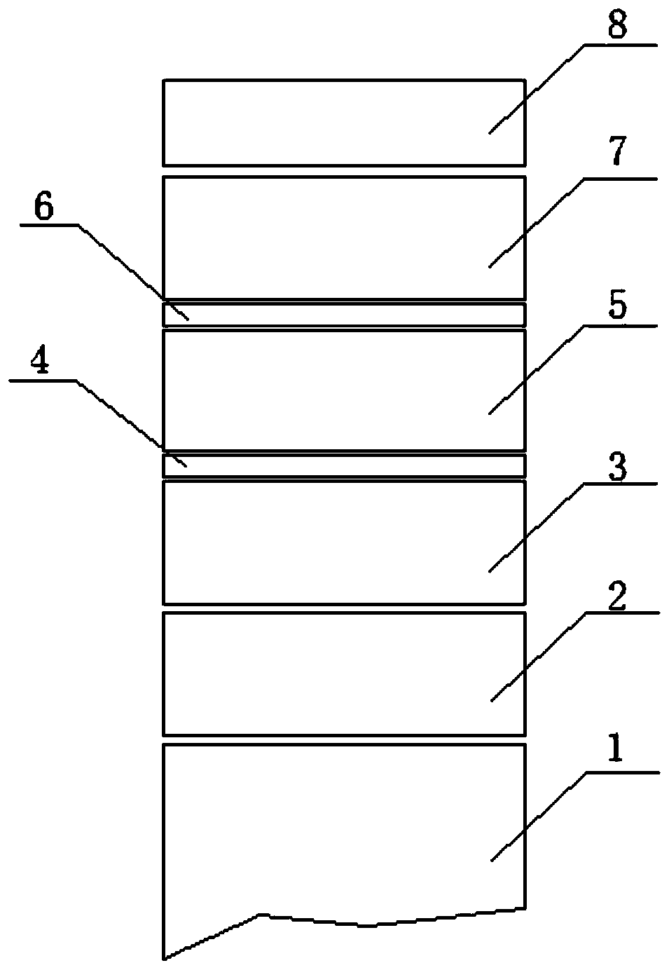
[0030] A method for preparing an LED wafer provided in this embodiment includes the following steps:

[0031] (1) growing an AlN composite substrate on a sapphire substrate;

[0032] (2) Epitaxial growth of a layer of Al on the AlN composite substrate 0.5 Ga 0.5 N quantum structure active layer;

[0033] (3) in Al 0.5 Ga 0.5 A very thin AlN buffer layer epitaxially on the N quantum structure active layer as a hole blocking layer;

[0034] (4) growing a multilayer quantum well structure on the AlN buffer layer;

[0035] (5) growing a P-type electron blocking layer on the quantum well structure;

[0036] (6) growing Mg-Siδ co-doped superlattice on the P-type electron blocking layer; ...


PUM

PropertyMeasurementUnit
thicknessaaaaaaaaaa
thicknessaaaaaaaaaa

Abstract

The invention provides an LED wafer and a preparation method thereof and an LED lamp. The preparation method comprises the following steps: 1) growing an AlN composite substrate on a sapphire substrate; 2) growing a layer of Al0.5Ga0.5N quantum structure active layer on the AlN composite substrate; 3) epitaxially growing a layer of thin AlN buffer layer on the Al0.5Ga0.5N quantum structure activelayer to serve as a hole blocking layer; 4) growing multiple layers of quantum well structures on the AlN buffer layer; 5) growing a P-type electron barrier layer on the quantum well structures; 6) growing Mg-Si[delta] co-doped superlattices on the P-type electron barrier layer; and 7) growing a layer of P<+>-GaN ohmic electrode cover layer on the Mg-Si[delta] co-doped superlattices. The beneficial effects are that, according to the preparation method of the LED wafer comprising a high-Al-component AlGaN epitaxial substrate, by growing the AlN composite substrate on the sapphire substrate, stress in the growth process is released effectively, and the high-quality AlGaN epitaxial substrate can be obtained.

Description

technical field [0001] The invention relates to an LED wafer, a preparation method thereof and an LED lamp. Background technique [0002] In the traditional LED crystal element preparation process, although the preparation of deep ultraviolet LED crystal element materials can be realized by adjusting the Al composition in the AlGaN material of the light-emitting layer, with the gradual increase of the Al composition in the AlGaN material, the AlGaN The difficulty from the epitaxial growth of the material to the fabrication of the device also increases. The specific manifestations are: with the increase of the Al composition, it is difficult to effectively control the two-dimensional growth during the epitaxial growth process, which easily leads to high defect density and uneven surface of the film. Polarity mixing and many other issues. [0003] In fact, the preparation of AlGaN epitaxial substrates with high Al composition is a key link in the production of deep ultraviole...

Claims


Application Information

Patent Timeline
Patent Type & Authority Patents(China)
IPC IPC(8): H01L33/06H01L33/00H01L21/02
CPCH01L21/0242H01L21/02458H01L21/0254H01L21/0262H01L33/007H01L33/0075H01L33/06
Inventor 邹国营高利辉于晓航
Owner ZHEJIANG SHUAIKANG ELECTRIC
Why Eureka
Try Eureka