
A three-dimensional plasmonic nanocomposite structure and its preparation method and application

A nanocomposite, plasma technology, applied in nanotechnology, nanotechnology, nanotechnology for materials and surface science, etc., can solve the problems of low utilization rate, low photoelectric conversion efficiency, etc. Utilization, the effect of enhancing the light absorption rate

Active Publication Date: 2021-10-08
HUAZHONG UNIV OF SCI & TECH +1
View PDF0 Cites 0 Cited by
  • Summary
  • Abstract
  • Description
  • Claims
  • Application Information

AI Technical Summary

Problems solved by technology

[0004] The invention provides a three-dimensional plasmonic nanocomposite structure and its preparation method and application, which are used to solve the technical problem of low photoelectric conversion efficiency caused by the low light utilization rate of the photosensitive layer in the existing photoelectric detection equipment

Method used


Image

  • A three-dimensional plasmonic nanocomposite structure and its preparation method and application
  • A three-dimensional plasmonic nanocomposite structure and its preparation method and application
  • A three-dimensional plasmonic nanocomposite structure and its preparation method and application

Examples


Embodiment 1

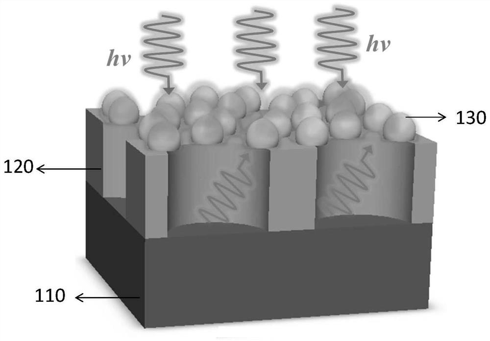
[0048] A three-dimensional plasmonic nanocomposite structure 100, such as figure 1As shown, it includes: an aluminum reflective layer 110 , an aluminum oxide array support 120 , and a gold nano-antenna 130 . The aluminum oxide array bracket is arranged on the aluminum reflection layer; the gold nano-antenna is arranged on the side surface of the aluminum oxide array bracket opposite to the aluminum reflection layer.

[0049] At present, most of the existing technologies use a single metal nano-antenna, and use the surface plasmon resonance effect to achieve a clamping effect on the incident light wave, thereby enhancing the light absorption rate of the light-affecting layer. Metal nanoantennas are affected by their normal size, so the optical coupling effect is limited, and the light transmission phenomenon is still serious. In order to prevent the overflow of incident light, this embodiment introduces an aluminum reflective layer and an aluminum oxide array resonant cavity, ...

Embodiment 2

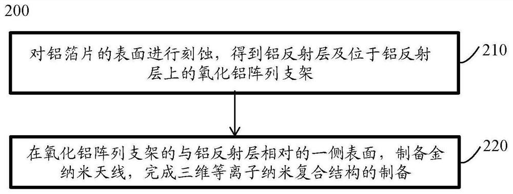
[0057] A method 200 for preparing a three-dimensional plasmonic nanocomposite structure as described in Embodiment 1, such as figure 2 shown, including:

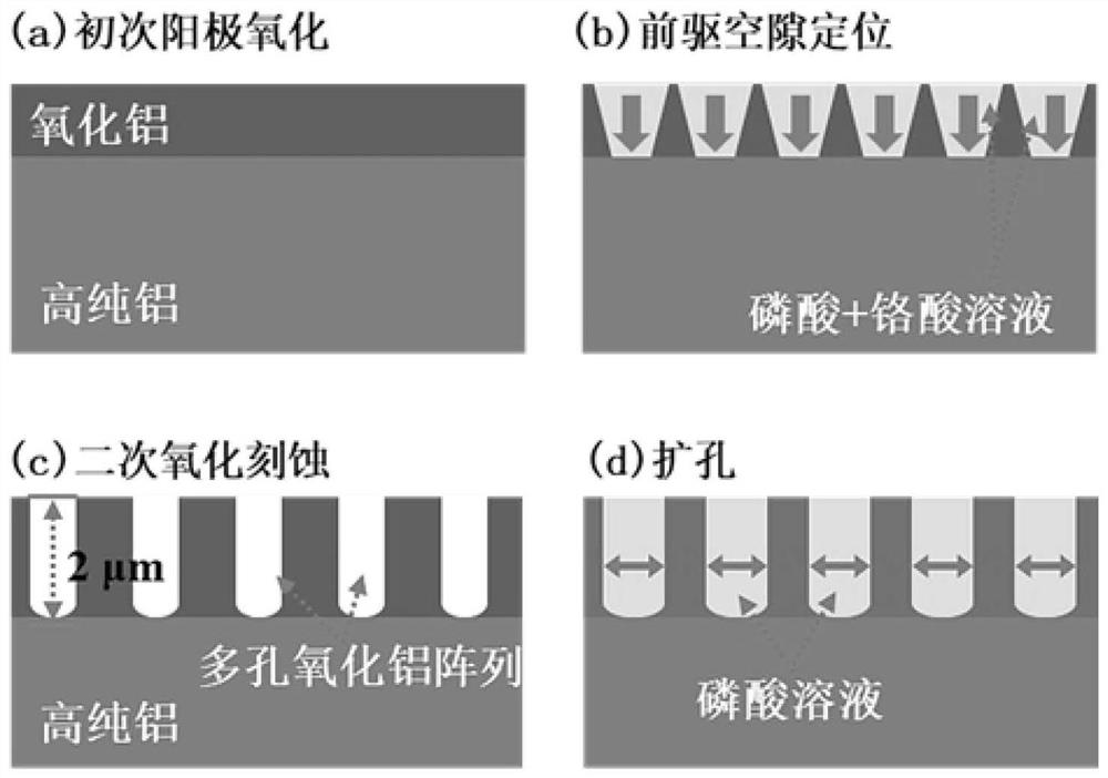
[0058] Step 210, etching the surface of the aluminum foil to obtain an aluminum reflective layer and an aluminum oxide array support located on the aluminum reflective layer;

[0059] Step 220 , preparing gold nano-antennas on the surface of the aluminum oxide array support opposite to the aluminum reflective layer, and completing the preparation of a three-dimensional plasmonic nano-composite structure.

[0060] It should be noted that the preparation method of the gold nano-antenna can be chemical synthesis method, photolithography method and the like.

[0061] In this embodiment, the aluminum oxide array support is prepared on the aluminum foil and the gold nano-antenna is prepared on the aluminum oxide array support to realize the combination of the aluminum oxide array support and the gold nano-antenna, so as to impro...

Embodiment 3

[0082] A photodetector 300, such as Figure 5 As shown, it includes: an electrode and a photosensitive layer stacked in sequence, and also includes: the three-dimensional plasma nanocomposite structure as described above, and the three-dimensional plasma nanocomposite structure is stacked on the side of the photosensitive layer opposite to the electrode.

[0083] The pore diameters of the periodic porous alumina arrays are respectively selected as 90 and 130 nm, and there are 6 samples in total, corresponding to different deposition thicknesses of the gold nanofilms. Such as Figure 6 Shown, the deposition thickness of gold nano film is respectively: Figure 6 (a)-(b) is 6nm, Figure 6 (c)-(d) are 10nm, Figure 6 (e)-(f) is 15nm; the apertures of alumina are: Figure 6 (a), (c), (e) are 90nm, Figure 6 (b), (d), and (f) are 130 nm.

[0084] Under each aperture, the self-assembled gold nanoantennas showed obvious size extension and shape irregularity with the gradual incr...


PUM

PropertyMeasurementUnit
thicknessaaaaaaaaaa
pore sizeaaaaaaaaaa
thicknessaaaaaaaaaa

Abstract

The invention discloses a three-dimensional plasma nanocomposite structure and its preparation method and application. The structure comprises: an aluminum reflection layer, an aluminum oxide array bracket, and a gold nanometer antenna. The aluminum oxide array bracket is arranged on the aluminum reflection layer; the gold nano-antenna is arranged on the side surface of the aluminum oxide array bracket opposite to the aluminum reflection layer. In order to prevent the overflow of the incident light, the present invention introduces the aluminum reflective layer and the aluminum oxide array resonant cavity, and combines the advantages of the aluminum reflective layer with strong light interference effect, the aluminum oxide array resonant cavity and the self-assembled gold nano antenna with strong surface plasmon effect, through The coupling effect of the reflective layer, the aluminum oxide array support and the gold nano-antenna can effectively clamp the light wave on the surface of the nanocomposite structure, realize the repeated utilization of the incident light wave, effectively improve the light utilization rate of the light-sensitive layer, and break through the light of traditional light detection materials. Absorption rate limitation.

Description

technical field [0001] The invention belongs to the technical field of optical devices, and in particular relates to a three-dimensional plasma nanocomposite structure and its preparation method and application. Background technique [0002] Photoelectric detection technology is a technology that uses light-sensitive materials to generate current in response to the characteristic band light waves radiated or reflected by the detected object, and then realizes the detection object recognition technology. With its fast response speed, high detection accuracy, large information capacity, non-contact, easy automation and integration and other advantages, it is widely used in military, medical, environmental monitoring and other fields. [0003] With the development of the semiconductor industry, miniaturized, lightweight, and low-power photoelectric detection equipment is greatly favored by portable equipment and weaponry because of its significant advantages in size, which grea...

Claims


Application Information

Patent Timeline
Patent Type & Authority Patents(China)
IPC IPC(8): H01L31/0232H01L31/08H01L31/18B82Y30/00B82Y40/00
CPCB82Y30/00B82Y40/00H01L31/02327H01L31/08H01L31/18Y02P70/50
Inventor 李明钰刘思思余慕妮苏东姜胜林张光祖
Owner HUAZHONG UNIV OF SCI & TECH
Learn More