A kind of p-type Aln thin film and its preparation method and application

A thin-film, p-type technology, applied in the direction of final product manufacturing, sustainable manufacturing/processing, electrical components, etc., can solve the problems of difficult breakthrough of AlN thin film and difficulty in activation of AlN thin film, and achieve good application prospects, good optical performance, and improved Effect of Crystal Quality

Active Publication Date: 2021-06-08
WUYI UNIV
View PDF0 Cites 0 Cited by
  • Summary
  • Abstract
  • Description
  • Claims
  • Application Information

AI Technical Summary

Problems solved by technology

[0003] AlN thin films have potential application value in the preparation of homojunction-based devices. However, due to the difficulty in the activation of AlN thin films, it has been difficult to break through high-quality p-type AlN thin films, which also makes optoelectronic devices based on AlN homojunctions in the initial stages of development

Method used


Image

  • A kind of p-type Aln thin film and its preparation method and application
  • A kind of p-type Aln thin film and its preparation method and application
  • A kind of p-type Aln thin film and its preparation method and application

Examples


Embodiment Construction

[0033] In order to describe the technical content, achieved objectives and effects of the present invention in detail, the following descriptions will be made in conjunction with the embodiments.

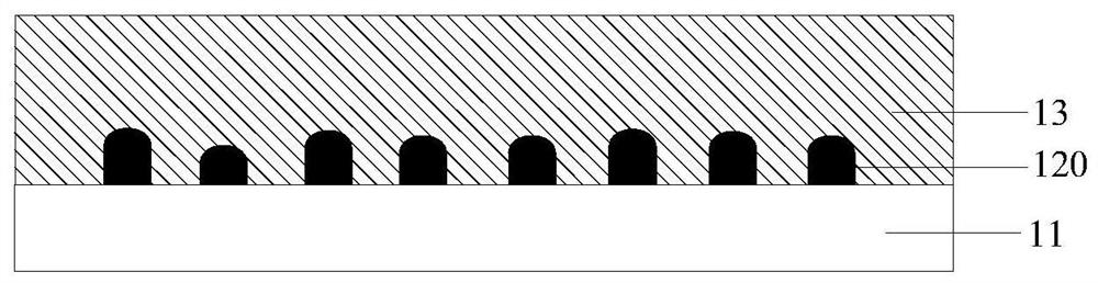
[0034] Embodiment 1 of the present invention is: a p-type AlN thin film, such as figure 1 As shown, its structure from bottom to top is a substrate 11 , a nanoparticle layer 120 (also called a PtLi layer) and an AlZnLiN thin film layer 13 . The specific steps are as follows:

[0035] (1) Firstly, a PtLi layer with a thickness of 10 nm is formed on the Si substrate 11 by sputtering method, followed by rapid annealing at 600° C. for 120 s to obtain a nanoparticle layer 120 with a diameter of 10-100 nm.

[0036] (2) A 150nm AlZnN film was grown at 200°C by magnetron sputtering, and kept at 900°C for 1h. During high-temperature growth or high-temperature annealing, Li atoms overflow into the AlZnN film layer, and co-dope AlN with Zn; activate Li and Zn doping during high-temperature a...


PUM

PropertyMeasurementUnit
thicknessaaaaaaaaaa
thicknessaaaaaaaaaa
thicknessaaaaaaaaaa

Abstract

The invention discloses a p-type AlN thin film and its preparation method and application. The structure of the thin film from bottom to top is a substrate, a PtLi or PtLi@PtLiO nano-dot layer and an AlZnLiN thin film layer. The preparation method comprises the following steps: S1, forming a PtLi layer on a substrate, annealing the PtLi layer to obtain a nanoparticle layer; S2, growing an AlZnN thin film layer on the substrate processed by the above steps, and (600-900) ° C and keep it warm for (0.5-12) h, Li atoms overflow into the AlZnN thin film layer, thereby obtaining the AlZnLiN thin film layer. The invention has ingenious scheme design, simple preparation and operation, and the prepared material has good crystal quality and optical performance.

Description

technical field [0001] The invention relates to the technical field of semiconductor materials, in particular to a p-type AlN thin film and its preparation method and application. Background technique [0002] AlN film is a wide bandgap semiconductor material, which has excellent chemical stability and good photoelectric and mechanical properties (such as good insulation, high piezoelectric coefficient and thermal conductivity, wide straight bandgap width, and fast acoustic wave propagation speed. , low thermal expansion coefficient, excellent mechanical strength, etc.), which makes it have broad application prospects in the fields of machinery, microelectronics, optics and electronic components, especially in the fields of ultraviolet light-emitting diodes (Light Emitting Diode, LED) and ultraviolet photodetectors. In preparation. [0003] AlN thin films have potential application value in the preparation of homojunction-based devices. However, due to the difficulty in the...

Claims


Application Information

Patent Timeline
Patent Type & Authority Patents(China)
IPC IPC(8): H01L31/0304H01L31/0352H01L31/103H01L31/18
CPCH01L31/03042H01L31/03044H01L31/035218H01L31/1035H01L31/1852H01L31/1856Y02P70/50
Inventor 杨为家王凤鸣关则毅何鑫
Owner WUYI UNIV
Why Eureka
Try Eureka