
LED packaging structure and method thereof

A technology of LED packaging and LED chips, applied in semiconductor devices, electrical components, circuits, etc., can solve the problems of reduced light intensity, reduced quantum efficiency of phosphors, and affected packaging lumen efficiency, so as to improve luminous dispersion and solve light transmittance. falling effect

Inactive Publication Date: 2018-03-23
XIAN CREATION KEJI CO LTD
View PDF4 Cites 1 Cited by
  • Summary
  • Abstract
  • Description
  • Claims
  • Application Information

AI Technical Summary

Problems solved by technology

Since the chip absorbs the backscattered light, this direct coating method will reduce the light extraction efficiency of the package
In addition, if the phosphor is directly coated on the chip, the high temperature generated by the chip will significantly reduce the quantum efficiency of the phosphor, which will seriously affect the lumen efficiency of the package.
[0007] 3. The safe junction temperature of the LED chip should be within 110°C. If the junction temperature is too high, it will lead to a series of problems such as reduced light intensity, spectral shift, increased color temperature, increased thermal stress, and accelerated aging of the chip, which will be greatly reduced. The service life of the LED is shortened, and at the same time, it can also cause accelerated aging of the encapsulation gel filled on the chip, affecting its light transmission efficiency

Method used


Image

  • LED packaging structure and method thereof
  • LED packaging structure and method thereof
  • LED packaging structure and method thereof

Examples


Embodiment 1

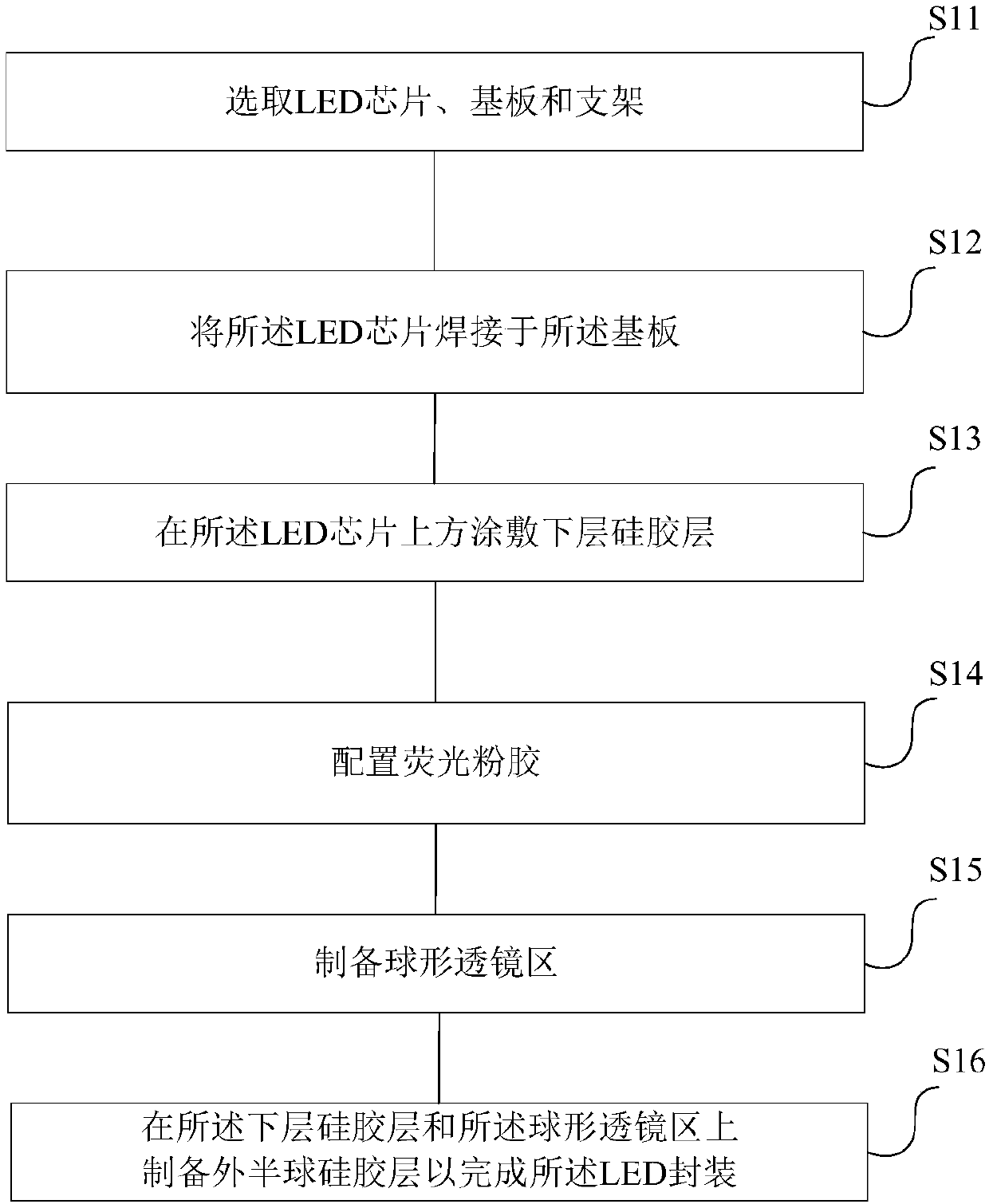
[0051] See figure 1 , figure 1 A schematic flow chart of an LED packaging method provided by an embodiment of the present invention, including:

[0052] S11, selecting LED chips and heat dissipation substrates;

[0053] S12. Welding the LED chip to the heat dissipation substrate;

[0054] S13. Coating a lower silica gel layer on the LED chip;

[0055] S14, configuring fluorescent powder glue;

[0056] S15, preparing a spherical lens area;

[0057] S16 , preparing an outer hemispherical silicone layer on the lower silicone layer and the spherical lens region to complete the LED package.

[0058] Preferably, step S12 may include:

[0059] S121, select a bracket;

[0060] S122, cleaning and drying the bracket and the heat dissipation substrate;

[0061] S123. Using a reflow soldering process, solder the LED chip to the heat dissipation substrate, and mount the heat dissipation substrate to the bracket.

[0062] Further, step S14 may include:

[0063] S141, selecting flu...

Embodiment 2

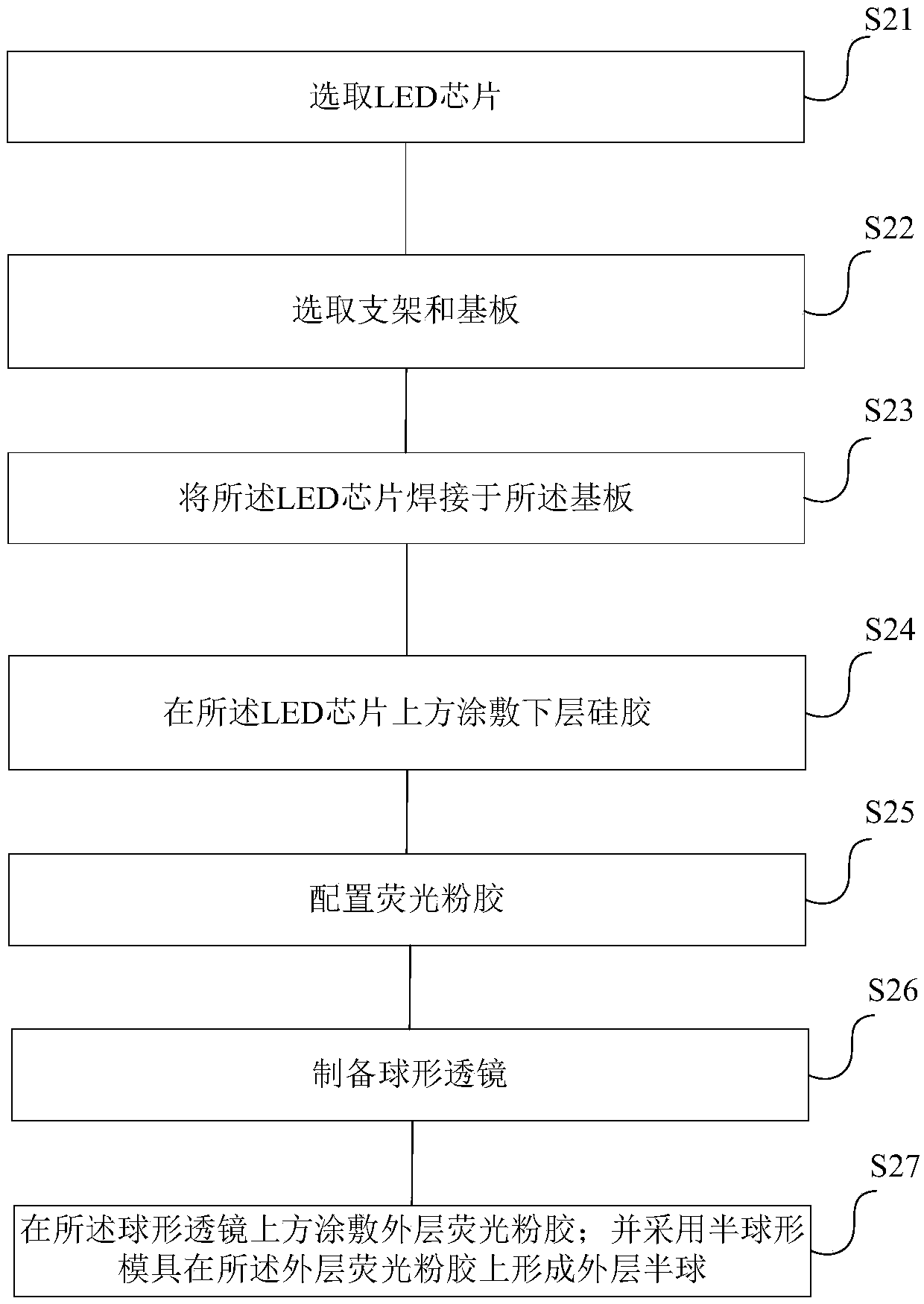
[0081] Please refer to figure 2 , figure 2 It is a flow chart of an LED packaging method provided by another embodiment of the present invention. On the basis of the above-mentioned embodiments, this embodiment describes the LED packaging method of the present invention in detail as follows. Specifically, include the following steps:

[0082] S21, selecting LED chips;

[0083] S22, selecting a bracket and a heat dissipation substrate;

[0084] S23. Welding the LED chip to the heat dissipation substrate;

[0085] S24. Coating a lower layer of silica gel above the LED chip;

[0086] S25, configuring fluorescent powder glue;

[0087] S26, preparing a spherical lens;

[0088] S27. Coating an outer phosphor glue on the spherical lens; and using a hemispherical mold to form an outer hemisphere on the outer phosphor glue; to complete the LED package.

[0089] Wherein, the refractive index of the lower layer of silica gel is lower than that of the outer layer of fluorescent p...

Embodiment 3

[0114] Further, please refer to Figure 6 , Figure 6 It is a schematic diagram of an LED package structure provided in another embodiment of the present invention. The LED package structure provided in this embodiment is prepared by the method provided in the above embodiment. Specifically, the LED packaging structure includes: an LED heat dissipation substrate 21 , a lower silica gel layer 22 , a spherical lens area 23 and an outer hemispherical silica gel layer 24 sequentially from bottom to top.

[0115] Wherein, the LED heat dissipation substrate 21 includes a heat dissipation substrate and LED chips disposed on the heat dissipation substrate.

[0116] Specifically, the lower silica gel layer 22 is silica gel without phosphor; wherein, the lower silica gel layer does not contain phosphor, which separates the phosphor from the LED chip, and solves the problem of decreasing quantum efficiency of the phosphor caused by high temperature.

[0117] Further, the spherical lens...


PUM

PropertyMeasurementUnit
Thicknessaaaaaaaaaa
Diameteraaaaaaaaaa

Abstract

The invention relates to an LED packaging structure and a method thereof. The method comprises steps: an LED chip, a cooling substrate and a bracket are selected; the LED chip is welded on the coolingsubstrate; a lower silica gel layer is applied above the LED chip; phosphor gel is prepared; a spherical lens area is manufactured; and an external hemisphere silica gel layer is prepared on the lower silica gel layer and the spherical lens area to complete LED packaging. The LED packaging method provided in the invention adopts a phosphor and LED chip separation process, and the problem that thequantum efficiency of the phosphor falls due to high temperature can be solved; the silica gel contacted with the LED chip is high temperature-resisting, and the problem that the transmittance fallsdue to aging and yellowing of the silica gel can be solved; and besides, silica gel balls are uniformly arranged in a rectangle or a diamond shape, and light of a light source can be ensured to be evenly distributed in a concentrated area.

Description

technical field [0001] The invention belongs to the technical field of LED packaging, and in particular relates to an LED packaging structure and a method thereof. Background technique [0002] A light-emitting diode (Light-Emitting Diode, LED) package refers to a package of a light-emitting chip, which is quite different from an integrated circuit package. The packaging of the LED is not only required to be able to protect the wick, but also to be able to transmit light. Due to the complex structure and process of high-power LED packaging, it directly affects the performance and life of the LED. [0003] Packaging is a key link in the preparation of white LEDs. The light-emitting mechanism of semiconductor materials determines that a single LED chip cannot emit white light with a continuous spectrum. Therefore, it is necessary to mix two or more complementary colors of light in the process to form white light. At present, the methods for realizing white LEDs are mainly Th...

Claims


Application Information

Patent Timeline
IPC IPC(8): H01L33/00H01L33/50H01L33/54H01L33/56
CPCH01L33/005H01L33/502H01L33/54H01L33/56
Inventor 张亮
Owner XIAN CREATION KEJI CO LTD
Learn More