Nitride semiconductor device
A technology of nitride semiconductors and semiconductors, which is applied in semiconductor devices, semiconductor/solid-state device manufacturing, transistors, etc., can solve problems such as difficulties in achieving high blocking withstand voltages, and achieve the effect of reducing on-resistance
- Summary
- Abstract
- Description
- Claims
- Application Information
AI Technical Summary
Problems solved by technology
Method used
Image

Examples
no. 1 Embodiment approach
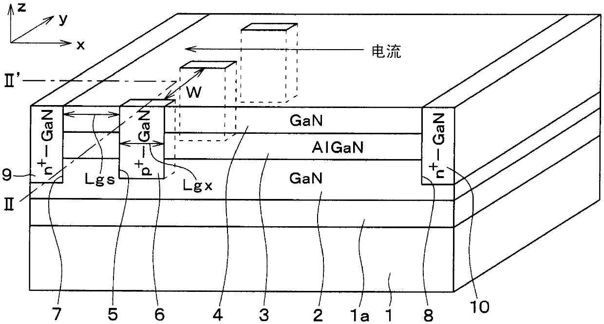
[0030] A first embodiment of the present invention will be described. In this embodiment mode, a nitride semiconductor device including a GaN device using a compound semiconductor mainly composed of GaN as a nitride semiconductor will be described.
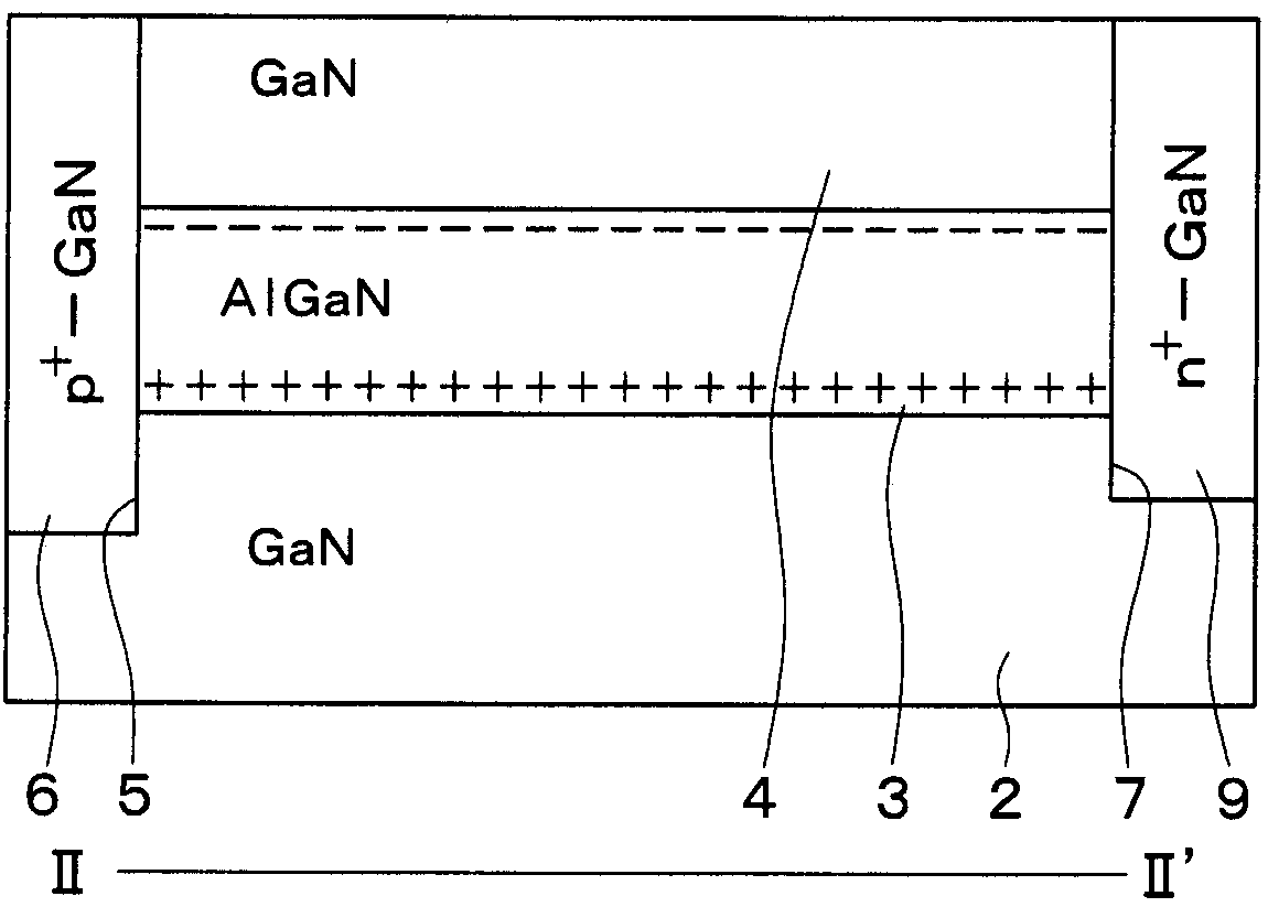
[0031] Such as figure 1 As shown, the nitride semiconductor device according to this embodiment includes a horizontal switching element. exist figure 1 In , only one cell of the switching element is shown, but actually, by using, for example, figure 1 The left end of the drawing is symmetrically arranged with the center line as the center line, and a plurality of units are formed to form a switching element. The switching element is set figure 1 Let the left-right direction be the x direction, let the depth direction be the y-direction, and let the up-down direction be the z-direction, and it is comprised as follows.
[0032] The horizontal switching element is formed using a structure in which a GaN layer 2 , an AlGaN la...
no. 2 Embodiment approach
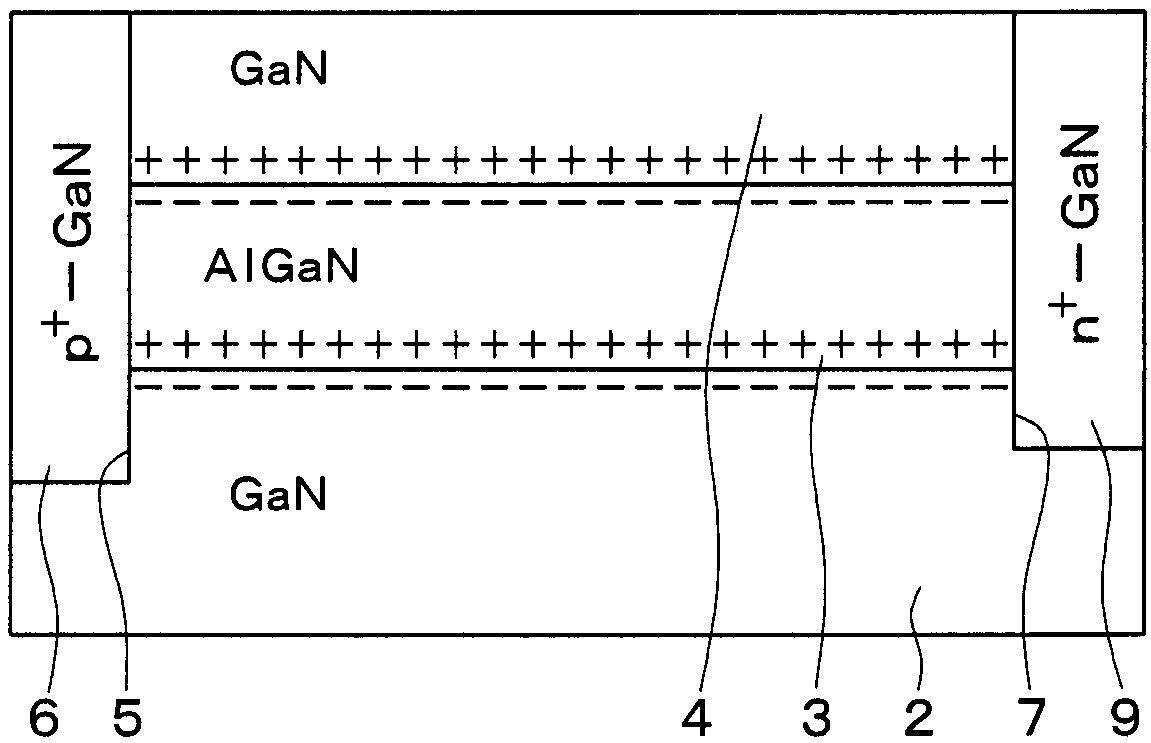
[0067] A second embodiment of the present invention will be described. In this embodiment, the structure of the compound semiconductor substrate, specifically, the structure of the channel formation layer is changed from that of the first embodiment. Regarding the rest, this embodiment is the same as the first embodiment, so only the parts different from the first embodiment will be described.
[0068] Such as Figure 5 As shown, in this embodiment, a compound semiconductor substrate is used as a compound semiconductor substrate in which multiple sets of AlGaN layers 3 and GaN layers 4 are stacked on top of GaN layer 2 formed on the surface of substrate 1 . The film thickness of the AlGaN layer 3 included in each group, that is, the z-direction dimension is set to be 10 nm to 200 nm, preferably 30 nm to 120 nm, as described in the first embodiment. Furthermore, the channel formation layer is constituted by a plurality of heterostructure structures formed of the AlGaN layer 3...
no. 3 Embodiment approach
[0073] A third embodiment of the present invention will be described. Compared with the first and second embodiments, this embodiment changes the p + - The structure of the GaN layer 6 . Regarding the rest, this embodiment is the same as the first and second embodiments, so only the parts different from the first and second embodiments will be described. In addition, here, p is changed with respect to the first embodiment + - The form of the structure of the GaN layer 6 is taken as an example, but the same structure can also be applied to the second embodiment.
[0074] Such as Figure 6A As shown, in this embodiment, it is made that p + - A structure in which the GaN layer 6 reaches the lowermost AlGaN layer 3 and does not reach the GaN layer 2 . Thus, in this embodiment, p + - The GaN layer 6 is formed in the middle of the AlGaN layer 3 on the lowermost layer side.
[0075] Even with such a structure, holes can be extracted and the electric field from the drain region...
PUM
 Abstract
Description
Claims
Application Information
 - R&D
- Intellectual Property
- Life Sciences
- Materials
- Tech Scout
- Unparalleled Data Quality
- Higher Quality Content
- 60% Fewer Hallucinations
Browse by: Latest US Patents, China's latest patents, Technical Efficacy Thesaurus, Application Domain, Technology Topic, Popular Technical Reports.
© 2025 PatSnap. All rights reserved.Legal|Privacy policy|Modern Slavery Act Transparency Statement|Sitemap|About US| Contact US: help@patsnap.com