Array substrate, organic light-emitting display panel, and display device

An array substrate and substrate substrate technology, which is applied to electrical components, electrical solid-state devices, circuits, etc., can solve the problems of incomplete data signal writing, affecting display uniformity, and large data signal transmission delay, so as to improve display uniformity. performance, avoid incomplete writing, and reduce the equivalent resistance

Inactive Publication Date: 2018-03-27
SHANGHAI TIANMA AM OLED
View PDF5 Cites 4 Cited by
  • Summary
  • Abstract
  • Description
  • Claims
  • Application Information

AI Technical Summary

Problems solved by technology

However, the resistance of the wiring formed by the heavily doped polysilicon semiconductor material is relatively large, which causes a large delay in the transmission of the data signal, resulting in a long time for writing the data signal, which in turn makes the writing of the data signal incomplete and affects the display uniformity.

Method used


Image

  • Array substrate, organic light-emitting display panel, and display device
  • Array substrate, organic light-emitting display panel, and display device
  • Array substrate, organic light-emitting display panel, and display device

Examples


Embodiment Construction

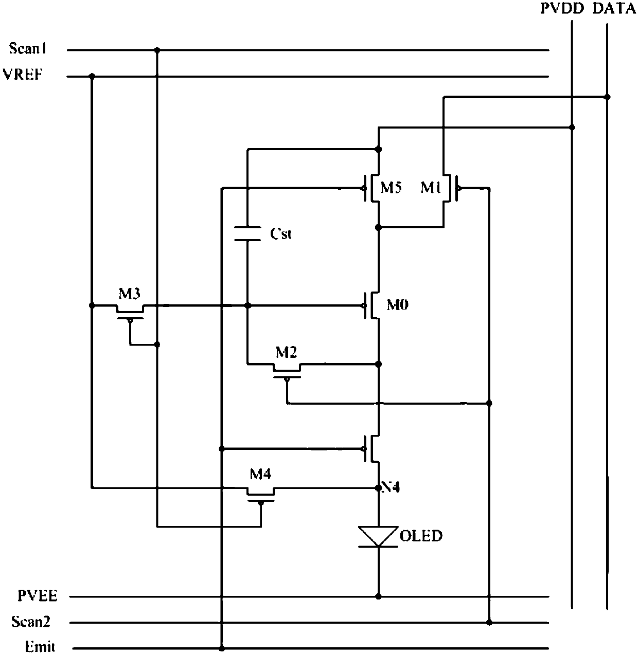
[0021] Such as figure 1 As shown, a specific structural schematic diagram of a pixel driving circuit is given. The pixel driving circuit includes: a driving transistor M0, a data transistor M1 connected between a data line DATA and the source of the driving transistor M0, a compensation transistor connected between the gate and the drain of the driving transistor M0 M2, an initialization transistor M3 connected between the gate of the driving transistor M0 and the reference signal line VREF, a reset transistor M4 connected between the reference signal line VREF and the anode of the organic light emitting diode OLED, and connected to the first power line The first light emission control transistor M5 between PVDD and the source of the driving transistor M0, the second light emission control transistor M6 connected between the drain of the driving transistor M0 and the anode of the organic light emitting diode OLED, and connected to The storage capacitor Cst between the gate of...


PUM


Abstract

The invention discloses an array substrate, an organic light-emitting display panel, and a display device. Metal bridge wires are set so as to enable the source electrodes of a data transistor and a drive transistor to be electrically connected with each other through one metal bridge wire, and enable the drain electrode of the drive transistor to be electrically connected with a compensation transistor through the other metal bridge wire. Moreover, the material of the metal bridge wires is metal, and the square resistance of the metal material is less than the square resistance of a heavily-doped semiconductor material, thereby reducing the equivalent resistance of the path that a data signal is inputted into a grid electrode of the drive transistor, reducing the delay of the data signal,and preventing the incomplete writing of the data signal. In particular, when the array substrate is used in a high-resolution display panel, the incomplete writing of the data signal is prevented, and the display uniformity is further improved.

Description

technical field [0001] The present invention relates to the field of display technology, in particular to an array substrate, an organic light emitting display panel and a display device. Background technique [0002] Organic Light Emitting Diode (OLED) is one of the hot spots in the field of flat panel display research today. Compared with Liquid Crystal Display (LCD), OLED display has low energy consumption, self-illumination, wide viewing angle and fast response speed. Etc. At present, OLED displays have begun to replace traditional LCD displays in display fields such as mobile phones, tablet computers, and digital cameras. Unlike LCDs that use a stable voltage to control brightness, OLEDs are driven by current and require a stable current to control their light emission. Generally, an OLED display drives the OLED to emit light through a driving transistor of a pixel driving circuit in its pixel. [0003] A general pixel driving circuit includes a plurality of transist...

Claims


Application Information

Patent Timeline
Patent Type & Authority Applications(China)
IPC IPC(8): H01L27/12H01L27/32
CPCH01L27/1244H10K59/131
Inventor 张鹏
Owner SHANGHAI TIANMA AM OLED
Why Eureka
Try Eureka