Pixel defining layer, preparation method thereof, and display panel

A pixel-defining layer and pixel-defining technology, which is applied in semiconductor/solid-state device manufacturing, electrical components, electric solid-state devices, etc., can solve problems affecting the light-emitting effect of the OLED light-emitting layer, affecting the life of the display device, and uneven thickness of the OLED light-emitting layer. , to achieve the effect of improving the light-emitting effect, increasing the life, and improving the uniformity of thickness

Active Publication Date: 2018-03-27
HEFEI XINSHENG OPTOELECTRONICS TECH CO LTD +1
View PDF4 Cites 11 Cited by
  • Summary
  • Abstract
  • Description
  • Claims
  • Application Information

AI Technical Summary

Problems solved by technology

In the inkjet printing process in the prior art, a dual-functional material with a small top surface energy and a large bottom surface energy is used as a pixel definition layer (PDL), and the surface energy of the top of the PDL is small so that it has a hydrophobic characteristics, which can limit the ink droplet of luminescent material in the light-emitting area, but the side of PDL is hydrophilic, which makes the ink droplet of luminescent material climb along the edge of PDL during the drying process, forming a thick edge and thin middle The thickness of the film layer, that is, the OLED light-emitting layer is uneven, which will affect the light-emitting effect of the OLED light-emitting layer and the life of the display device

Method used


Image

  • Pixel defining layer, preparation method thereof, and display panel
  • Pixel defining layer, preparation method thereof, and display panel
  • Pixel defining layer, preparation method thereof, and display panel

Examples


Embodiment Construction

[0029] Embodiments of the present application provide a pixel defining layer, a preparation method thereof, and a display panel, which are used to improve the film thickness uniformity of the OLED light-emitting layer, improve the light extraction effect of the OLED light-emitting layer, and increase the life of the display device.

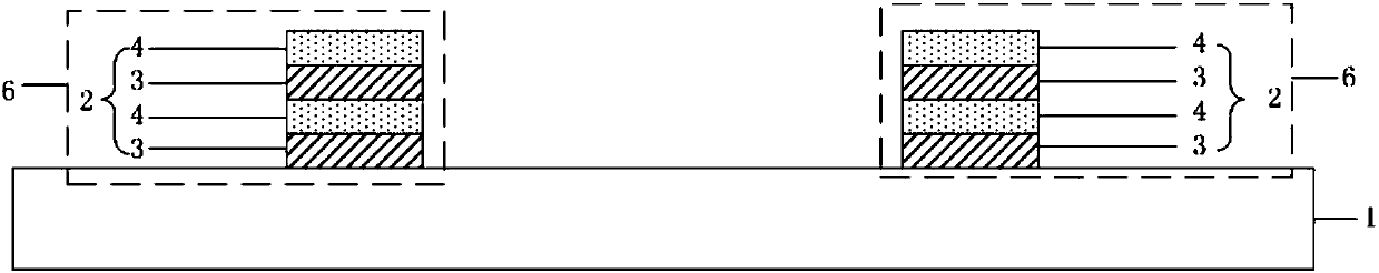
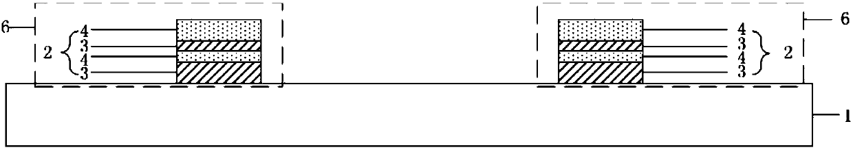
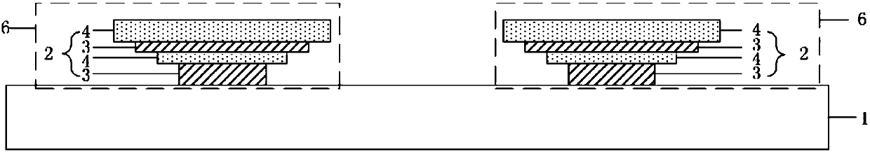
[0030] A pixel definition layer provided by the embodiment of the present application, such as figure 1 As shown, the pixel defining layer 6 is disposed on the substrate 1, and the pixel defining layer 1 includes: on the substrate 1, at least four layers of pixel defining layers are alternately stacked by hydrophilic pixel defining layers 3 and hydrophobic pixel defining layers 4. Layer 2; the pixel defining sublayer 2 adjacent to the substrate 1 is a hydrophilic pixel defining layer 3, and in the direction perpendicular to the substrate 1, the pixel defining sublayer 2 farthest from the substrate 1 is a hydrophobic pixel defining layer 4

[0031...


PUM


Abstract

The present invention discloses a pixel defining layer, a preparation method thereof and a display panel. The invention aims to improve the film formation uniformity of an OLED (Organic Light EmittingDiode) light emitting layer, improve the light emitting effect of the OLED light emitting layer, and prolong the service life of a display device. The pixel defining layer provided by one embodimentof the present invention is disposed on a substrate; the pixel defining layer comprises at least four pixel defining sub-layers which are composed of hydrophilic pixel defining layers and hydrophobicpixel defining layers which are alternately stacked on the substrate; the pixel defining sub-layer adjacent to the substrate is a hydrophilic pixel defining layer; and in a direction perpendicular tothe substrate, the pixel defining sub-layer farthest from the substrate is a hydrophobic pixel defining layer.

Description

technical field [0001] The present application relates to the field of display technology, in particular to a pixel defining layer, a preparation method thereof, and a display panel. Background technique [0002] Organic Light-Emitting Diode (OLED) is an electroluminescent device, which has the advantages of self-luminescence, high luminous efficiency, low operating voltage, light and thin, flexible and simple manufacturing process, and is widely used in display lighting and other fields. At present, there are two ways to form the light-emitting layer in OLEDs. One is the evaporation process, which is most suitable for the production of small-sized OLEDs and has been mass-produced; the other is the solution process. This method mainly uses The prepared organic material solution is used to form a film by spin coating, inkjet printing or screen printing. This method has the advantages of low cost, high production capacity, and is suitable for large-size panels, and has been wi...

Claims


Application Information

Patent Timeline
Patent Type & Authority Applications(China)
IPC IPC(8): H01L27/32H01L51/56
CPCH10K59/122H10K71/00
Inventor 胡月王欣欣彭锐廖金龙
Owner HEFEI XINSHENG OPTOELECTRONICS TECH CO LTD
Why Eureka
Try Eureka