Array substrate, manufacturing method of array substrate and display appliance
A technology for array substrates and substrates, which is applied in the field of array substrates and display devices, can solve the problem of high power consumption, achieve the effect of improving image quality and reducing power consumption
- Summary
- Abstract
- Description
- Claims
- Application Information
AI Technical Summary
Problems solved by technology
Method used
Image


Examples
Embodiment Construction
[0034] In order to further explain the technical means and effects adopted by the present invention to achieve the intended invention purpose, the specific implementation, structure, features and effects of the present invention will be described in detail below in conjunction with the accompanying drawings and preferred embodiments.
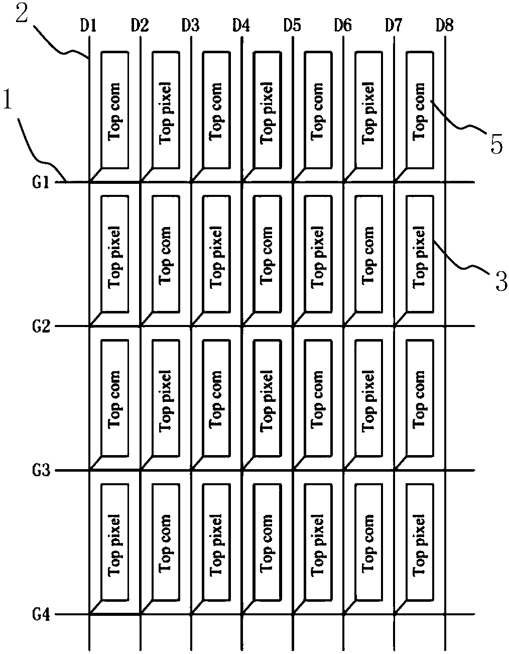
[0035] figure 1 It is a schematic structural diagram of an array substrate in an embodiment of the present invention. figure 2 It is a schematic cross-sectional view of two adjacent pixel units of an array substrate at an oxide thin film transistor in an embodiment of the present invention. Such as figure 1 and figure 2As shown, the array substrate of the present invention includes a substrate 4 and a gate line (Gate line) 1 and a data line (Date line) 2 arranged on the substrate 4, and the gate line 1 and the data line 2 are arranged to cross each other to form pixels arranged in a matrix Each pixel unit is provided with an oxide thin film...
PUM
 Abstract
Description
Claims
Application Information