CXP modular structure

A module structure and metal block technology, which is applied in light guides, optics, instruments, etc., can solve the problems of poor module adaptability to the environment, module performance degradation, and low product qualification rate, so as to prevent performance degradation, improve product reliability, and increase The effect of cooling area

Inactive Publication Date: 2018-04-13
JIANGSU ALLRAY
View PDF3 Cites 4 Cited by
  • Summary
  • Abstract
  • Description
  • Claims
  • Application Information

AI Technical Summary

Problems solved by technology

However, due to the high level of integration, various heating elements inside the module are concentrated, resulting in heat concentration, causing module performance degradation or even damage
Inside the module, the driver chip of the laser and the amplifier chip of the detector are the main heating elements. The conventional CXP module places the driver chip of the laser and the amplifier chip of the detector on the same PCB (printed circuit board), and then passes The ground layer and vias on the PCB conduct heat to one end of the housing for heat dissipation. The disadvantage of this solution is that the heat is concentrated, and the module adapts to the environment poorly
Moreover, once any components are damaged during the production process, maintenance will be difficult and the product qualification rate will be low.

Method used


Image

  • CXP modular structure
  • CXP modular structure
  • CXP modular structure

Examples


Embodiment Construction

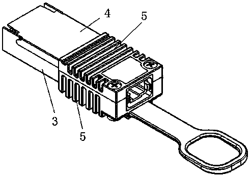
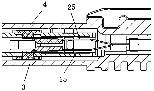
[0018] see Figure 1 to Figure 4 , a CXP module structure, including an upper shell 4 and a lower shell 3, the upper shell 4 and the lower shell 3 are locked by screws, and the optical port ends of the upper shell 4 and the lower shell 3 are blade-type structures 5, increasing the entire shell heat dissipation area.

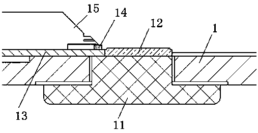
[0019] The lower shell 3 is provided with a transmitting terminal printed circuit board 1, and the transmitting terminal printed circuit board 1 is provided with a transmitting terminal metal block mounting hole (not shown in the figure), and a transmitting terminal metal block mounting hole is provided with a transmitting terminal metal block 11. The end metal block 11 is a "convex"-shaped structure, and the top of the transmitting end metal block 11 is a raised portion. A driver chip 12 is pasted on the surface of the top surface of the body. Specifically, the driver chip 12 is pasted with the metal block 11 of the transmitting end through thermal conductive g...


PUM


Abstract

The invention relates to a CXP modular structure comprising an upper casing and a lower casing. The lower casing is provided therein with a transmitting end printed circuit board in which a transmitting end metal block is disposed. A driver chip is pasted on the surface of the transmitting end metal block by a thermally conductive adhesive. A transmitting end ceramic spacer is pasted on the surface of the transmitting end printed circuit board. A laser array chip is pasted on the surface of the transmitting end ceramic spacer. A gap between the transmitting end metal block and the lower casingis filled with the thermally conductive adhesive. A receiving end printed circuit board is arranged in the upper casing, and a receiving end metal block is arranged in the receiving end printed circuit board. An amplifier chip is pasted on the surface of the receiving end metal block by the thermal conductive adhesive. A receiving end ceramic spacer is pasted on the surface of the receiving end printed circuit board. A detector array chip is pasted on the surface of the receiving end ceramic spacer. A gap between the receiving end metal block and the upper casing is filled with the thermallyconductive adhesive. The CXP modular structure has a good heat dissipation effect and can increase the working environment temperature of an optical device by more than 10 degrees centigrade.

Description

technical field [0001] The invention relates to the field of communication equipment, in particular to a CXP module structure. Background technique [0002] With its advantages of high speed, large capacity, anti-interference, low energy consumption and strong confidentiality, photoelectric communication technology has been widely used in the fields of sensing detection, communication transmission, data storage, biomedicine, aerospace and other fields. It is an important supporting technology for the construction of modernization and national defense industry. [0003] The CXP (12-channel small-volume pluggable) module integrates 24 optical fiber channels, and the rate of a single channel can reach more than 10Gbps at present, and the receiving and sending rate of the module can reach 120Gbps, which has great data transmission capacity. However, due to the high level of integration, various heating elements inside the module are concentrated, resulting in heat concentration...

Claims


Application Information

Patent Timeline
Patent Type & Authority Applications(China)
IPC IPC(8): G02B6/42
CPCG02B6/4246G02B6/4268
Inventor 薛京谷缪玉筛于佩
Owner JIANGSU ALLRAY
Why Eureka
Try Eureka