Thin film transistor, preparation method thereof, array substrate and display device

A thin-film transistor and array substrate technology, applied in the display field, can solve the problems of excessive parasitic capacitance of TFT, poor light stability, low device mobility, etc., and achieve the effects of reducing resistance, improving yield, and simplifying the manufacturing process

Pending Publication Date: 2018-04-13
BOE TECH GRP CO LTD
View PDF9 Cites 6 Cited by
  • Summary
  • Abstract
  • Description
  • Claims
  • Application Information

AI Technical Summary

Problems solved by technology

[0002] In order to produce a display panel with a higher resolution, it is necessary to solve the problem of excessive parasitic capacitance of the TFT. In the prior art, a top-gate self-aligned TFT structure is generally used to reduce the parasitic capacitance of the TFT.
However, the display panel with the top-gate TFT structure faces the following two problems to be solved. On the one hand, how to reduce the resistance between the active layer and the source-drain electrodes, refer to figure 1 , in order to reduce the contact resistance between the active layer and the source and drain, in the prior art, the area where the active layer 03 contacts the source and drain electrodes 02 is generally treated with gas plasma such as Ar and He, that is,

Method used


Image

  • Thin film transistor, preparation method thereof, array substrate and display device
  • Thin film transistor, preparation method thereof, array substrate and display device
  • Thin film transistor, preparation method thereof, array substrate and display device

Examples


Example Embodiment

[0053] In order to make the above objectives, features and advantages of the present invention more obvious and understandable, the present invention will be further described in detail below with reference to the accompanying drawings and specific embodiments.
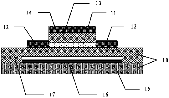
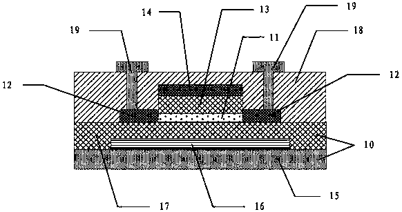
[0054] In an embodiment of this application, refer to figure 2 , Shows a schematic cross-sectional structure of a thin film transistor, the thin film transistor may include: a substrate 10 and an active layer 11 and a first source drain electrode 12 disposed on the substrate 10, the first source drain electrode 12 and the active layer 11 connection; the first insulating layer 13 and the gate 14 are stacked on the active layer 11, and the gate 14 has the same thickness and material as the first source and drain electrodes 12.

[0055] Specifically, the active layer 11 is the active layer, including an active region or a channel region, and the material may be amorphous silicon, low-temperature polysilicon or metal oxide mat...


PUM


Abstract

The invention provides a thin film transistor, a preparation method thereof, an array substrate and a display device. The thin film transistor comprises a substrate, an active layer and a first source-drain electrode, wherein the active layer and the first source-drain electrode are arranged on the substrate. The first source-drain electrode is connected with the active layer. The first source-drain electrode in direct contact with the active layer is arranged, wherein a gate and the first source-drain electrode share the same thickness and material. Compared with the prior art, the thin filmtransistor has the advantages that an LDD region between the first source-drain electrode and the active layer is not needed; the total resistance between the source-drain electrode and the active layer no longer includes the resistance of the LDD region; and the resistance between the source-drain electrode and the active layer is effectively reduced. The first source-drain electrode can effectively shield side light, which can further improve the TFT illumination stability. Due to the fact that the gate and the first source-drain electrode share the same thickness and material, the gate andthe first source-drain electrode can be simultaneously formed. The preparation process is simplified. The yield is improved. The cost is reduced.

Description

technical field [0001] The invention relates to the field of display technology, in particular to a thin film transistor, a preparation method thereof, an array substrate and a display device. Background technique [0002] In order to manufacture a display panel with a higher resolution, it is necessary to solve the problem of excessive parasitic capacitance of the TFT. In the prior art, a top-gate self-aligned TFT structure is generally used to reduce the parasitic capacitance of the TFT. However, the display panel with the top-gate TFT structure faces the following two problems to be solved. On the one hand, how to reduce the resistance between the active layer and the source-drain electrodes, refer to figure 1 , in order to reduce the contact resistance between the active layer and the source and drain, in the prior art, the area where the active layer 03 contacts the source and drain electrodes 02 is generally treated with gas plasma such as Ar and He, that is, the LDD i...

Claims


Application Information

Patent Timeline
IPC IPC(8): H01L29/786H01L29/49H01L29/45H01L21/336H01L21/34
CPCH01L29/45H01L29/4908H01L29/66757H01L29/66969H01L29/78633H01L29/78666H01L29/78675H01L29/7869H01L27/1225H01L27/1262H01L29/41733H01L27/1288H01L29/66742H01L29/78621
Inventor 王国英宋振
Owner BOE TECH GRP CO LTD
Why Eureka
Try Eureka