Supercharge Your Innovation With Domain-Expert AI Agents!

Semiconductor structure and forming method therefor

一种半导体、栅极结构的技术,应用在半导体结构及其形成领域,能够解决半导体器件电学性能有待提高等问题,达到改善栅漏电流问题的效果

Active Publication Date: 2018-05-08
SEMICON MFG INT (SHANGHAI) CORP +1
View PDF6 Cites 3 Cited by
  • Summary
  • Abstract
  • Description
  • Claims
  • Application Information

AI Technical Summary

Problems solved by technology

[0004] Although the introduction of high-K metal gates can improve the electrical properties of semiconductor devices to a certain extent, the electrical properties of semiconductor devices formed in the prior art still need to be improved.

Method used


Image

  • Semiconductor structure and forming method therefor
  • Semiconductor structure and forming method therefor
  • Semiconductor structure and forming method therefor

Examples


Embodiment Construction

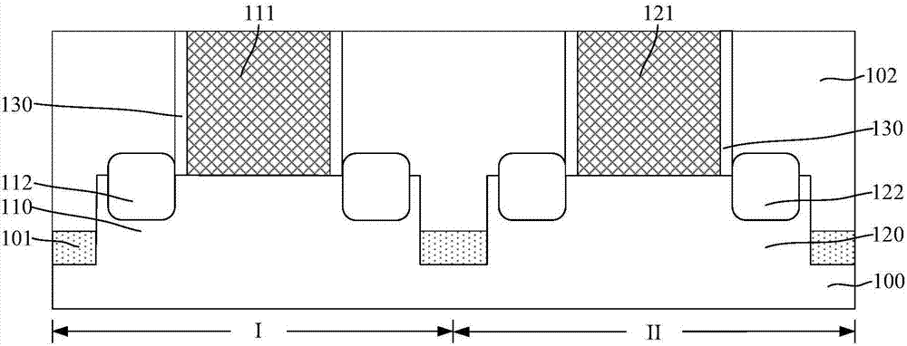
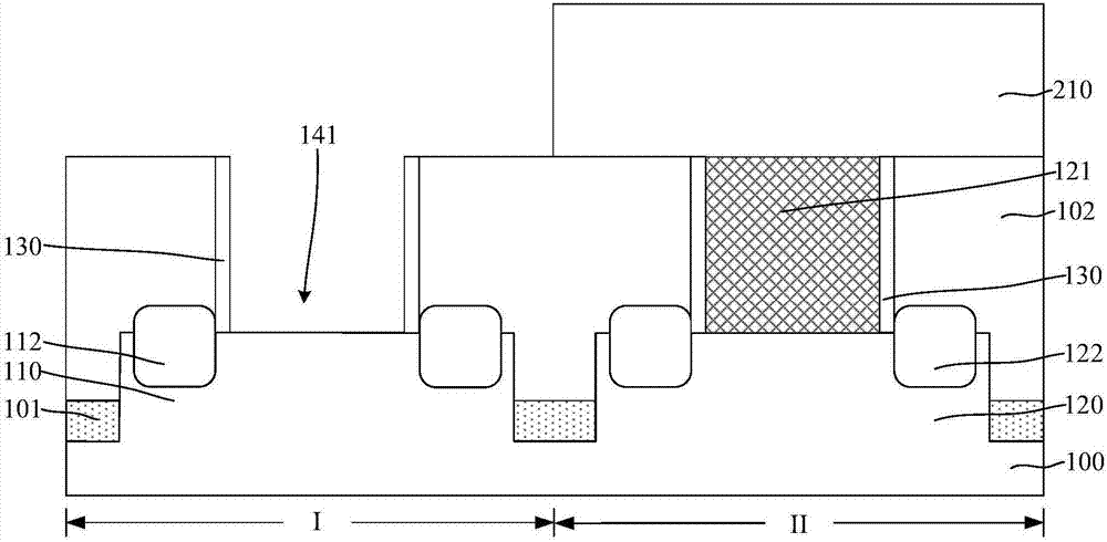
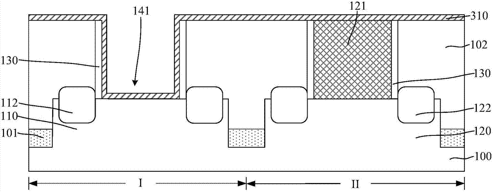
[0012] It can be seen from the background technology that with the continuous reduction of semiconductor device technology nodes, high-k gate dielectric materials are currently used instead of traditional silicon dioxide gate dielectric materials to improve semiconductor gate leakage current (Gate Leakage) and equivalent gate oxide thickness (EOT )And other issues. However, the electrical performance of semiconductor devices still needs to be improved. Combined with a method of forming a semiconductor structure, the reason is analyzed.

[0013] The forming method includes: providing a substrate, the substrate includes an NMOS region and a PMOS region, the NMOS region substrate is a III-V group compound substrate, and the PMOS region substrate is a germanium-containing substrate; using an oxidation process, the substrate is forming an interface layer on the interface layer; forming a high-K gate dielectric layer on the interface layer; forming a metal layer on the high-K gate ...


PUM

PropertyMeasurementUnit
annealing pointaaaaaaaaaa

Abstract

The invention discloses a semiconductor structure and a forming method therefor, and the method comprises the steps: providing a substrate which comprises an NMOS region and a PMOS region, wherein thesubstrate in the NMOS region is a III-V group compound substrate, and the substrate in the PMOS region is a germanium-containing substrate; forming a first high-K gate medium layer on the substrate in the NMOS region; forming an interface layer on the substrate in the PMOS region through the oxidation technology; forming a second high-K gate medium on the interface layer and the first high-K gatemedium layer; and forming a metal layer on the second high-K gate medium layer. According to the invention, the thickness of the second high-K gate medium layer can be adjusted to solve a problem ofa gate leakage current of the PMOS region. The equivalent gate oxide thickness of the NMOS region is enabled to solve a problem of a gate leakage current of the NMOS region through the adjustment of the thickness of the first high-K gate medium layer.

Description

technical field [0001] The invention relates to the field of semiconductors, in particular to a semiconductor structure and a forming method thereof. Background technique [0002] The main semiconductor device of integrated circuits, especially VLSIs, is metal-oxide-semiconductor field effect transistors (MOS transistors). With the continuous development of integrated circuit manufacturing technology, the technology nodes of semiconductor devices continue to decrease, and the geometric dimensions of semiconductor devices follow Moore's law. When the size of semiconductor devices is reduced to a certain extent, various secondary effects brought about by the physical limits of semiconductor devices appear one after another, and it becomes more and more difficult to scale down the feature size of semiconductor devices. Among them, in the field of semiconductor manufacturing, how to solve the problem of large leakage current of semiconductor devices is the most challenging. Th...

Claims


Application Information

Patent Timeline
Patent Type & Authority Applications(China)
IPC IPC(8): H01L21/8258H01L27/092
CPCH01L21/8258H01L27/092H01L29/66795H01L29/785H01L29/66545H01L29/517H01L29/513H01L21/02112H01L21/02236H01L21/02255H01L21/28255H01L21/28264H01L21/823814H01L21/823821H01L21/823828H01L21/823857H01L27/0924H01L29/16H01L29/20H01L29/42364H01L29/518
Inventor 李勇
Owner SEMICON MFG INT (SHANGHAI) CORP
Features
  • R&D
  • Intellectual Property
  • Life Sciences
  • Materials
  • Tech Scout
  • Unparalleled Data Quality
  • Higher Quality Content
  • 60% Fewer Hallucinations
Learn More