Reconfigurable radio frequency and microwave power amplifier

A microwave power and power amplification technology, applied in power amplifiers, high-frequency amplifiers, improving amplifiers to expand bandwidth, etc., can solve the problems of increasing the bandwidth of amplifier modules, increasing the complexity and cost of RF front-end, high linearity and efficiency, etc.

Pending Publication Date: 2018-05-08
牛旭
View PDF0 Cites 21 Cited by
  • Summary
  • Abstract
  • Description
  • Claims
  • Application Information

AI Technical Summary

Problems solved by technology

[0003] At present, 2G wireless communication terminals need saturated power amplifiers, 3G/4G/5G terminals need linear power amplifiers, and 3G/4G/5G terminals need linear power amplifiers that need to meet the fundamental wave required by the frequency band in different channels and different bands Impedance and harmonic load impedance required by class F power amplifier, which makes the linearity and power added efficiency of the power amplifier module as a linear power amplifier low
In addition, although the 3G/4G/5G frequency band covers

Method used


Image

  • Reconfigurable radio frequency and microwave power amplifier
  • Reconfigurable radio frequency and microwave power amplifier
  • Reconfigurable radio frequency and microwave power amplifier

Examples


Embodiment 1

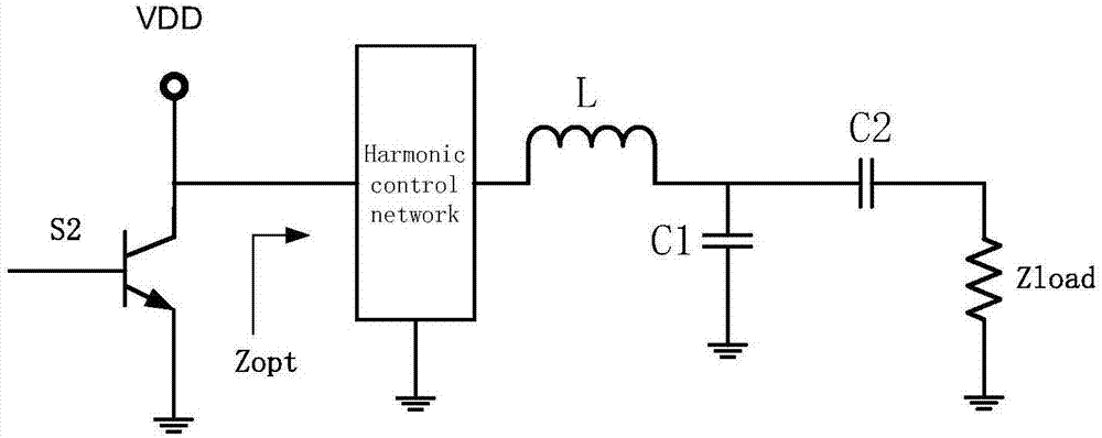
[0092] Figure 10 so Figure 9 Based on the load matching structure in , the structural diagram of reconstructing the inductance in the adjustable output matching network is shown in Figure 9 Among them, for the entire bandwidth of MB 1710MHz~2025MHz, the range of required capacitance C1 is 11.3pF~13.3pF, the minimum value is 11.3pF, then the Figure 9 Capacitor C1 in the reconstruction, that is, as Figure 10 As shown, the design and capacitor C are reserved on the RF switch chip 11 Parallel capacitor C 12 Series RF switch S 1 , and with capacitance C 11 Parallel capacitor C 13 Series RF switch S 2 , capacitance C 12 and capacitance C 13 For reconstruction, the capacitor C 11 It is implemented with a fixed-value SMD capacitor. Real-time control of S through control signals from bias and control circuits 1 , S 2 on or off to achieve capacitance C 12 and capacitance C 13 Whether the two capacitors are connected or not. Capacitance C 11 =11.3pF, realized by SMD...

Embodiment 2

[0095] Figure 11 so Figure 9 A structural schematic diagram of reconstructing the inductance in the adjustable output matching network based on the load matching structure in Figure 9 For the whole bandwidth of MB 1710MHz~2025MHz, the required inductance L 2 The variation range is 1.67nH~2.0nH, then it can be Figure 9 The inductance L in 2 to refactor, such as Figure 11 shown, the inductance L 21 =2nH, use substrate wound inductor or SMD inductor, inductance L 22 = 23nH and inductance L 23 =18nH adopts wire winding or SMD inductor on the RF switch chip, : inductance L 22 and inductance L 23 for refactoring. where the inductance L 22 = 23nH series RF switch S 3 , the reconstructed inductance L 23 = 18nH series RF switch S 4 , when S 3 , S 4 When both are disconnected, only the inductance L 21 =2nH access matching network; connect S 3 while disconnecting S 4 , the inductance L can be obtained 21 , inductance L 22 In parallel structure, the equivalent ind...

Embodiment 3

[0098] Figure 12 so Figure 9 Based on the load matching structure in , another structure diagram for reconstructing the inductance in the adjustable output matching network is shown in Figure 9 For the whole bandwidth of MB 1710MHz~2025MHz, the required inductance L 2 The variation range is 1.67nH~2.0nH, then it can be Figure 9 The inductance L in 2 to refactor, such as Figure 12 shown, the inductance L 21 =1.67nH, capacitance CL 22 =0.4pF series RF switch S 3 , capacitance CL 23 =0.4pF series RF switch S 4 , capacitance CL 22 and capacitance CL 23 For reconstruction, the inductance L 21 Using substrate wound inductors or SMD inductors, capacitor CL 22 , capacitor CL 23 Using MIM capacitors on the RF switch chip. When S 3 , S 4 are disconnected, only L 21 =1.67nH connected to the matching network, this inductance value is most suitable for use when the amplifier works in band34 (2010~2025MHz); connect S 3 , S 4 When one of the switches, the inductance L...


PUM


Abstract

The invention relates to a reconfigurable radio frequency and microwave power amplifier. The reconfigurable radio frequency and microwave power amplifier comprises an input radio frequency switch, anadjustable input matching network, a power amplifier stage, an adjustable output matching network and an output radio frequency switch which are connected in turn, and an adjustable harmonic impedancecontrol network and a bias and control circuit; and the adjustable input matching network and the adjustable output matching network respectively comprise at least one LC network with a fundamental wave impedance conversion function, wherein the LC network comprises at least one reconfigurable device, and the reconfigurable device is connected with a passive device in the LC network in parallel.According to the reconfigurable radio frequency and microwave power amplifier provided by the invention, the reconfigurable harmonic impedance control network and the fundamental wave impedance matching network are realized through the adjustable input matching network, the adjustable harmonic impedance control network and the adjustable output matching network; and when a power amplifier works indifferent bands of a linear power amplifier mode, a load impedance network can be reconfigured in real time, which satisfies the fundamental wave impedance and harmonic load required by each frequency band.

Description

technical field [0001] The invention relates to the field of mobile communication, in particular to a reconfigurable radio frequency and microwave power amplifier. Background technique [0002] In the field of mobile communication represented by smart phones, radio frequency and microwave power amplifier (poweramplifier module, referred to as PA Module, or PAM, hereinafter referred to as RF power amplifier or power amplifier) ​​is a very important component in the communication terminal, and its performance is directly It affects the quality of mobile communication, and directly determines the service life of a single charge of mobile communication terminal equipment. RF engineers and chip design engineers must continuously improve the performance of power amplifiers while controlling or reducing the complexity and cost of RF front-ends. [0003] At present, 2G wireless communication terminals need saturated power amplifiers, 3G / 4G / 5G terminals need linear power amplifiers,...

Claims


Application Information

Patent Timeline
IPC IPC(8): H03F3/20H03F3/189H03F1/42
CPCH03F1/42H03F3/189H03F3/20
Inventor 牛旭
Owner 牛旭
Why Eureka
Try Eureka