Manufacturing method of probes

A manufacturing method and probe technology, which are used in the manufacture of measuring instruments, measuring devices, instruments, etc., to achieve the effects of high precision, small needle diameter and consistent needle shape

Active Publication Date: 2018-05-11
浙江微针半导体有限公司
View PDF4 Cites 2 Cited by
  • Summary
  • Abstract
  • Description
  • Claims
  • Application Information

AI Technical Summary

Problems solved by technology

[0003] At present, as the pixels of liquid crystal display panels are getting higher and higher, the requirements for probes such as the miniaturization of the needle body and the shape of the needle body are also increasing, and the traditional mechanical processing methods can no longer meet the requirements.

Method used


Image

  • Manufacturing method of probes
  • Manufacturing method of probes
  • Manufacturing method of probes

Examples


Embodiment Construction

[0026] The following will clearly and completely describe the technical solutions in the embodiments of the present invention with reference to the accompanying drawings in the embodiments of the present invention. Obviously, the described embodiments are only some, not all, embodiments of the present invention. All other embodiments obtained by persons of ordinary skill in the art based on the embodiments of the present invention belong to the protection scope of the present invention.

[0027] The probes of the present invention are not limited to the testing of liquid crystal display panels, and other probe cards such as integrated circuit testing, or probe structures that need to be manufactured with tiny dimensions can be implemented. The embodiments described below are for illustration only, and therefore the scope of the present invention is not limited thereto.

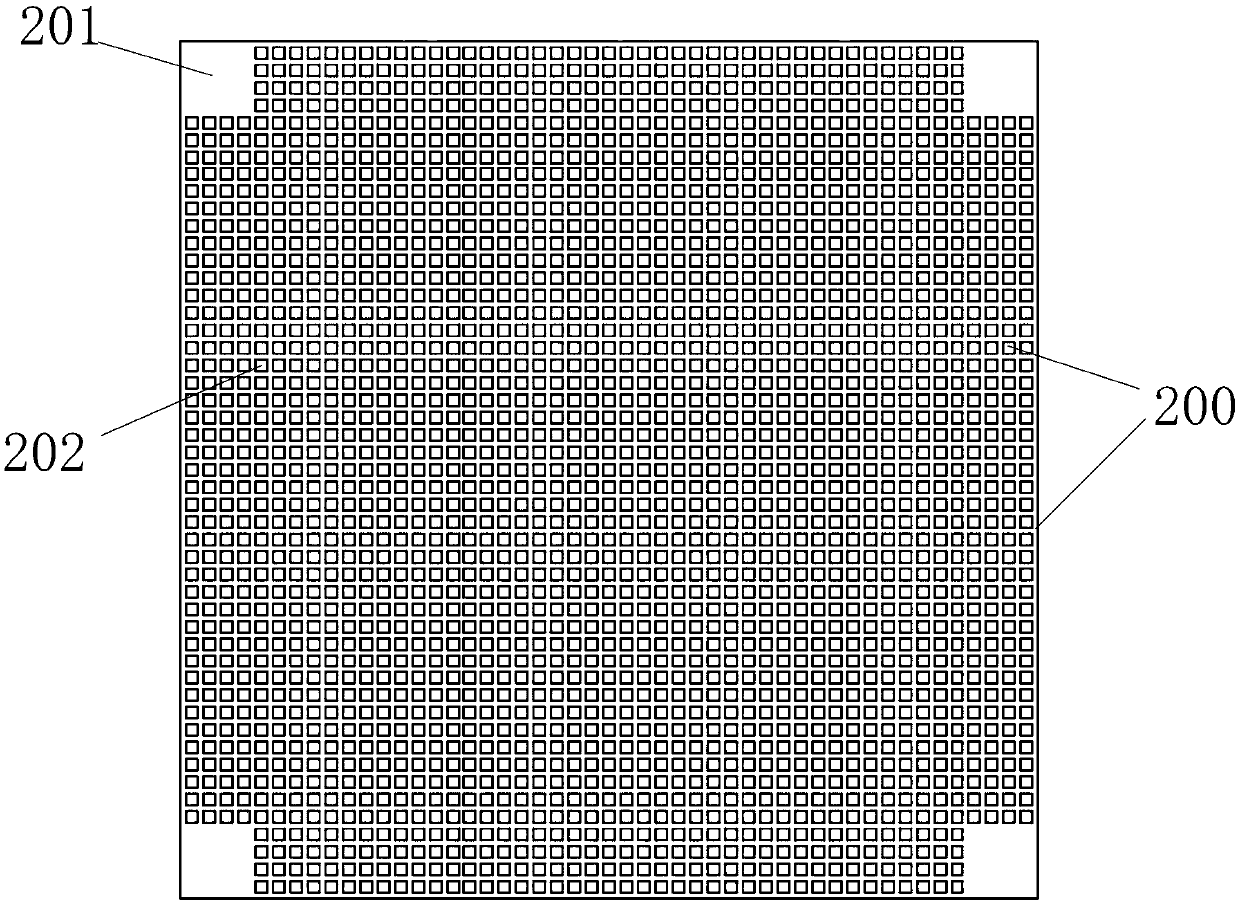
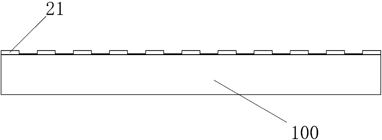
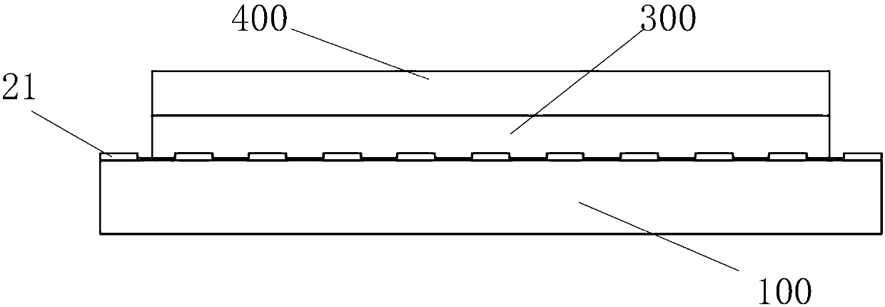
[0028] Such as Figure 1-8 Shown, according to the manufacturing method of a kind of probe of the present ...


PUM


Abstract

The invention discloses a manufacturing method of a probe. Each probe is composed of a probe post and a probe cone. The manufacturing method comprises: a metal layer is formed on a substrate, whereinthe metal layer consists of a base layer and a conductive circuit layer formed by a plurality of patterns on the base layer; probe posts and probe cone model holes are formed on the patterns and integrated moulding is realized by electroplating. According to the manufacturing method, the restriction from the traditional mechanical processing capability is eliminated; while equal-ratio batched probe body manufacturing in a fixed area, the parallelism between the probes is ensured and the height error is reduced. Moreover, all probes are formed by integrated moulding; and after the batched production, the probe models are consistent, the probe diameter is small, the probe body has the shorter length, and the precision is improved.

Description

technical field [0001] The invention relates to the related technical field of integrated circuit probe card and display panel detection, in particular to a method for manufacturing a probe. Background technique [0002] A probe (Probe) is a device used to measure the electrical characteristics of tiny electronic components (for example, semiconductor components or thin-film transistor arrays in liquid crystal display panels). As is well known in the art, a thin-film transistor array ( ThinFilmTransistorArray, TFTArray) has a plurality of gate lines and signal lines connected to a plurality of test pads (TestPad) for exchanging signals with an external electronic system; the thin film transistor array is for electrical signals input through these test pads Processing is performed, and the processed results are transmitted to an external system through the test pads to detect the quality or defects of the electrical characteristics of the display panel. [0003] At present, ...

Claims


Application Information

Patent Timeline
IPC IPC(8): G01R3/00
CPCG01R3/00
Inventor 刘红军杨文仁
Owner 浙江微针半导体有限公司
Why Eureka
Try Eureka