Deposition method of magnetic thin film lamination layer, magnetic thin film lamination layer and micro inductor device

A technology of magnetic thin film and deposition method, which is applied in the field of microelectronics, can solve the problems that the magnetic film stack is not easy to be thick, the workpiece to be processed cracks and falls off, and the micro-inductance device cannot be used, so as to broaden the application frequency range and avoid cracks Shedding effect

Active Publication Date: 2018-05-11
BEIJING NAURA MICROELECTRONICS EQUIP CO LTD
View PDF12 Cites 0 Cited by
  • Summary
  • Abstract
  • Description
  • Claims
  • Application Information

AI Technical Summary

Problems solved by technology

[0004] But in above-mentioned magnetic film lamination, because magnetic film layer tensile stress is big, matter is brittle, the above-mentioned magnetic film lamination obtained by this magnetic film layer is difficult to do thick, and if the above-mentioned magnetic film lamination total thickness of preparation surpasses 500nm, Due to the large tensile stress and brittle characteristics of the magnetic film layer, the magnetic film laminate has a large tensile stress, and the above-mentioned magnetic film laminate will fall off and the attached workpiece (or cracks and fall off) will appear, and it cannot be used for the preparation of Micro-inductance device
In addition, because the above-mentioned magnetic film stack is not easy to make thick, the thickness of the prepared above-mentioned magnetic film stack is small, so the application frequency range of the inductance device prepared by it is only 1-5 GHz, and cannot cover the frequency range of MHz

Method used


Image

  • Deposition method of magnetic thin film lamination layer, magnetic thin film lamination layer and micro inductor device
  • Deposition method of magnetic thin film lamination layer, magnetic thin film lamination layer and micro inductor device
  • Deposition method of magnetic thin film lamination layer, magnetic thin film lamination layer and micro inductor device

Examples


Embodiment Construction

[0050] In order for those skilled in the art to better understand the technical solution of the present invention, the method for depositing the magnetic thin film stack and the magnetic thin film stack provided by the present invention will be described in detail below in conjunction with the accompanying drawings.

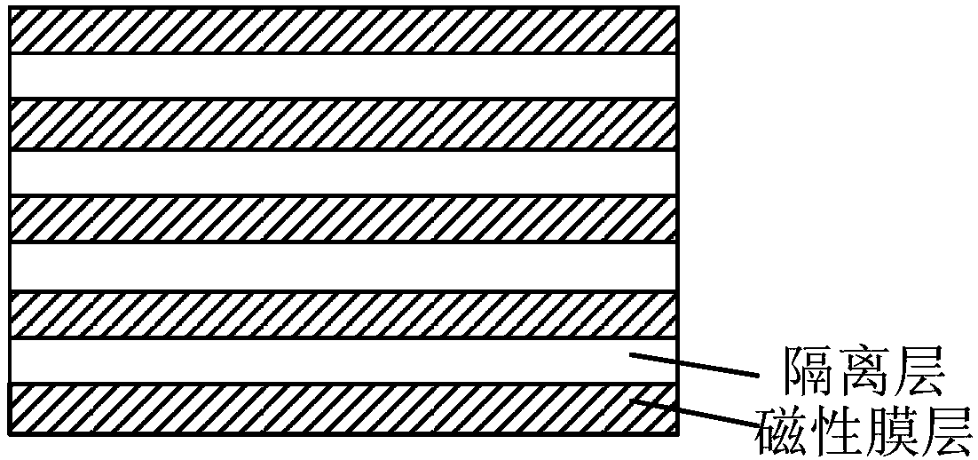
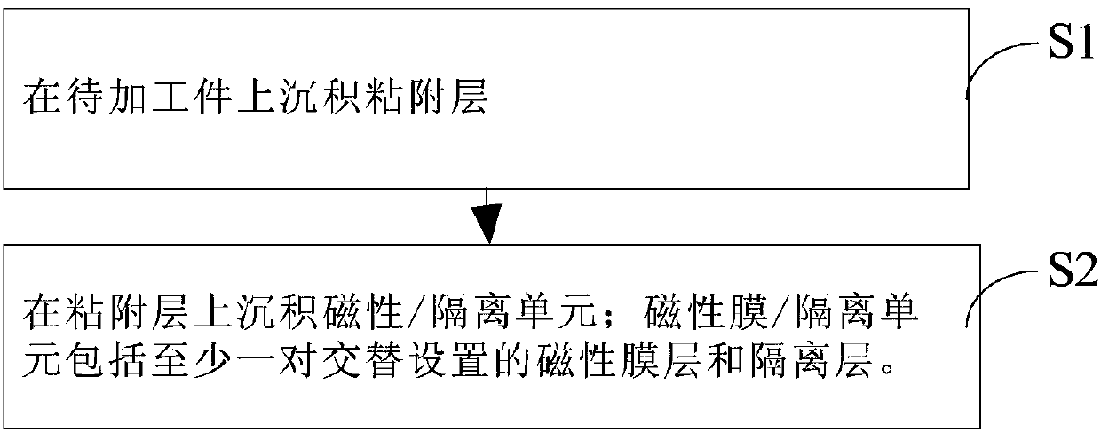
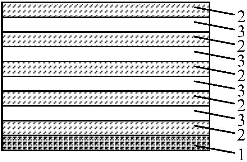
[0051] figure 2 It is a flow chart of the deposition method of the magnetic thin film stack provided by the first embodiment of the present invention. image 3 It is a structure diagram of a magnetic thin film stack obtained by using the deposition method of the magnetic thin film stack provided in the first embodiment of the present invention. Please also refer to figure 2 with image 3 , the deposition method of magnetic thin film lamination, it comprises the following steps:

[0052] S1, depositing an adhesion layer 1 on the workpiece to be processed;

[0053] S2 , depositing a magnetic / isolation unit on the adhesion layer 1 , the magnetic / isolation unit i...


PUM

PropertyMeasurementUnit
thicknessaaaaaaaaaa
thicknessaaaaaaaaaa
thicknessaaaaaaaaaa

Abstract

The invention provides a deposition method of a magnetic thin film lamination layer, the magnetic thin film lamination layer and a micro inductor device. The deposition method comprises the followingsteps of S1, depositing an adhesive layer on a workpiece to be processed; and S2, depositing a magnetic/isolation unit, wherein the magnetic/isolation unit comprises at least one pair of magnetic filmlayer and isolation layer which are alternatively arranged. With the deposition method of the magnetic thin film lamination layer, provided by the invention, the total thickness of the magnetic thinfilm lamination layer can be increased, so that the application frequency range of the inductor device fabricated by the method can be expanded.

Description

technical field [0001] The invention relates to the technical field of microelectronics, in particular to a deposition method of a magnetic thin film stack, a magnetic thin film stack and a micro-inductance device. Background technique [0002] With the development of science and technology, the integrated circuit manufacturing process can significantly reduce the size of the processor, but there are still some core components such as integrated inductors and noise suppressors that face many challenges in terms of high frequency, miniaturization, and integration. difficulty. In order to solve this problem, soft magnetic thin film materials with high magnetization, high magnetic permeability, high resonance frequency and high resistivity have attracted more and more attention. [0003] figure 1 It is a structural diagram of an existing magnetic thin film stack. Such as figure 1 As shown, the magnetic film stack is composed of alternately arranged isolation layers and magn...

Claims


Application Information

Patent Timeline
Patent Type & Authority Applications(China)
IPC IPC(8): H01F41/18H01F10/14H01F17/00C23C14/34C23C14/35
CPCC23C14/3485C23C14/35H01F10/14H01F17/0013H01F41/18H01F10/30H01F41/32H01F3/02H01F17/04H01F27/263H01F41/0206H01F41/14
Inventor 杨玉杰丁培军张同文夏威王厚工
Owner BEIJING NAURA MICROELECTRONICS EQUIP CO LTD
Why Eureka
Try Eureka