Semiconductor structure and formation method thereof

A technology of semiconductor and gate structure, which is applied in the field of semiconductor structure and its formation, can solve the problems that the electrical performance of semiconductor devices needs to be improved, and achieve the effect of optimizing electrical performance

Inactive Publication Date: 2018-05-11
SEMICON MFG INT (SHANGHAI) CORP +1
View PDF4 Cites 5 Cited by
  • Summary
  • Abstract
  • Description
  • Claims
  • Application Information

AI Technical Summary

Problems solved by technology

[0004] Although the introduction of high-k metal gates can improve the electrical performance of semiconductor devices to a certain extent, the electrical performance of semiconductor devices formed by the prior art still needs to be improved.

Method used


Image

  • Semiconductor structure and formation method thereof
  • Semiconductor structure and formation method thereof
  • Semiconductor structure and formation method thereof

Examples


Embodiment Construction

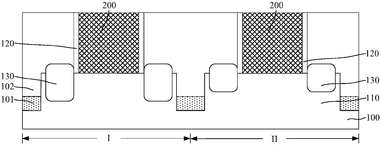
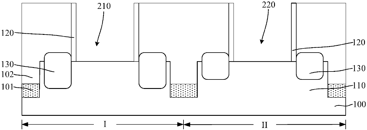
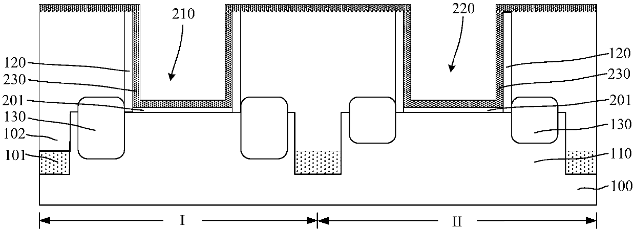
[0031] It can be seen from the background art that the electrical performance of semiconductor devices still needs to be improved. Combined with a method of forming a semiconductor structure, the reason is analyzed.

[0032] The forming method includes: providing a substrate; forming an interlayer dielectric layer on the substrate; forming an opening exposing the substrate in the interlayer dielectric layer; forming a gate dielectric layer on the bottom and side walls of the opening Forming a work function layer on the gate dielectric layer; forming a capping layer on the work function layer; forming a metal layer filling the opening on the capping layer; the gate dielectric layer in the opening, the work function layer, capping layer and metal layer are used to form the gate structure.

[0033] Wherein, the metal layer usually contains F ions that are easy to diffuse. In order to prevent the F ions from diffusing into the work function layer of the gate structure, a capping ...


PUM


Abstract

The invention relates to a semiconductor structure and a formation method thereof. The formation method comprises the steps of providing a substrate; forming a gate dielectric layer on the substrate;forming a work function layer on the gate dielectric layer; forming a cap layer on the work function layer, wherein the cap layer comprise a Ti layer; and forming a metal layer on the cap layer, wherein the gate dielectric layer, the work function layer, the cap layer and the metal layer are used for forming a gate structure. According to the invention, the cap layer is formed o the work functionlayer before the metal layer is formed, the cap layer comprises the Ti layer, the metal layer generally contains easily diffused F ions, and the F ion is high in electronegativity and easy to be boundwith a Ti ion to form a titanium-fluorine bond. Correspondingly, the Ti ions can well adsorb the F ions. Therefore, the Ti layer can effectively play a role of preventing diffusion of the F ions, sothat the F ions are avoided from being diffused to the work function layer, and thus influences imposed on a work function value of the work function layer are avoided.

Description

technical field [0001] The invention relates to the field of semiconductors, in particular to a semiconductor structure and a forming method thereof. Background technique [0002] The main semiconductor device of an integrated circuit, especially a very large scale integrated circuit, is a metal-oxide-semiconductor field effect transistor (MOS transistor). With the continuous development of integrated circuit manufacturing technology, the technology nodes of semiconductor devices continue to decrease, and the geometric dimensions of semiconductor devices follow Moore's law. When the size of semiconductor devices is reduced to a certain extent, various secondary effects caused by the physical limits of semiconductor devices appear one after another, and it becomes more and more difficult to scale down the feature size of semiconductor devices. Among them, in the field of semiconductor manufacturing, the most challenging thing is how to solve the problem of large leakage curr...

Claims


Application Information

Patent Timeline
Patent Type & Authority Applications(China)
IPC IPC(8): H01L21/8238H01L21/336H01L29/78H01L29/49H01L27/092
CPCH01L21/823821H01L21/823828H01L27/0924H01L29/4966H01L29/66795H01L29/785
Inventor 杨晓蕾王安妮
Owner SEMICON MFG INT (SHANGHAI) CORP
Why Eureka
Try Eureka