Semiconductor structures and methods of forming them

A technology of semiconductor and metal gate, applied in the field of semiconductor structure and its formation, can solve the problem that the electrical performance of semiconductor devices needs to be improved, and achieve the effect of optimizing the electrical performance

Active Publication Date: 2020-06-09
SEMICON MFG INT (SHANGHAI) CORP +1
View PDF3 Cites 0 Cited by
  • Summary
  • Abstract
  • Description
  • Claims
  • Application Information

AI Technical Summary

Problems solved by technology

[0004] Although the introduction of high-k metal gates can improve the electrical performance of semiconductor devices to a certain extent, the electrical performance of semiconductor devices formed in the prior art needs to be improved

Method used


Image

  • Semiconductor structures and methods of forming them
  • Semiconductor structures and methods of forming them
  • Semiconductor structures and methods of forming them

Examples


Embodiment Construction

[0014] It can be seen from the background art that the electrical performance of semiconductor devices formed in the prior art needs to be improved. The reason is analyzed in conjunction with a method of forming a semiconductor structure, the method of forming includes:

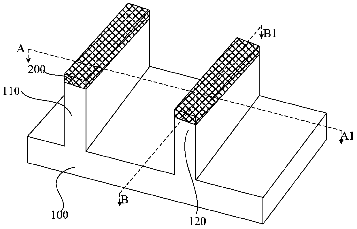
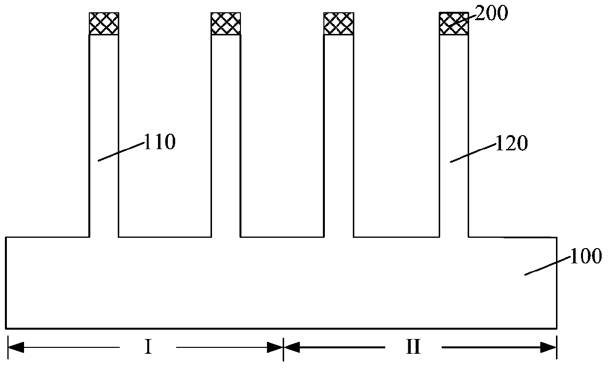
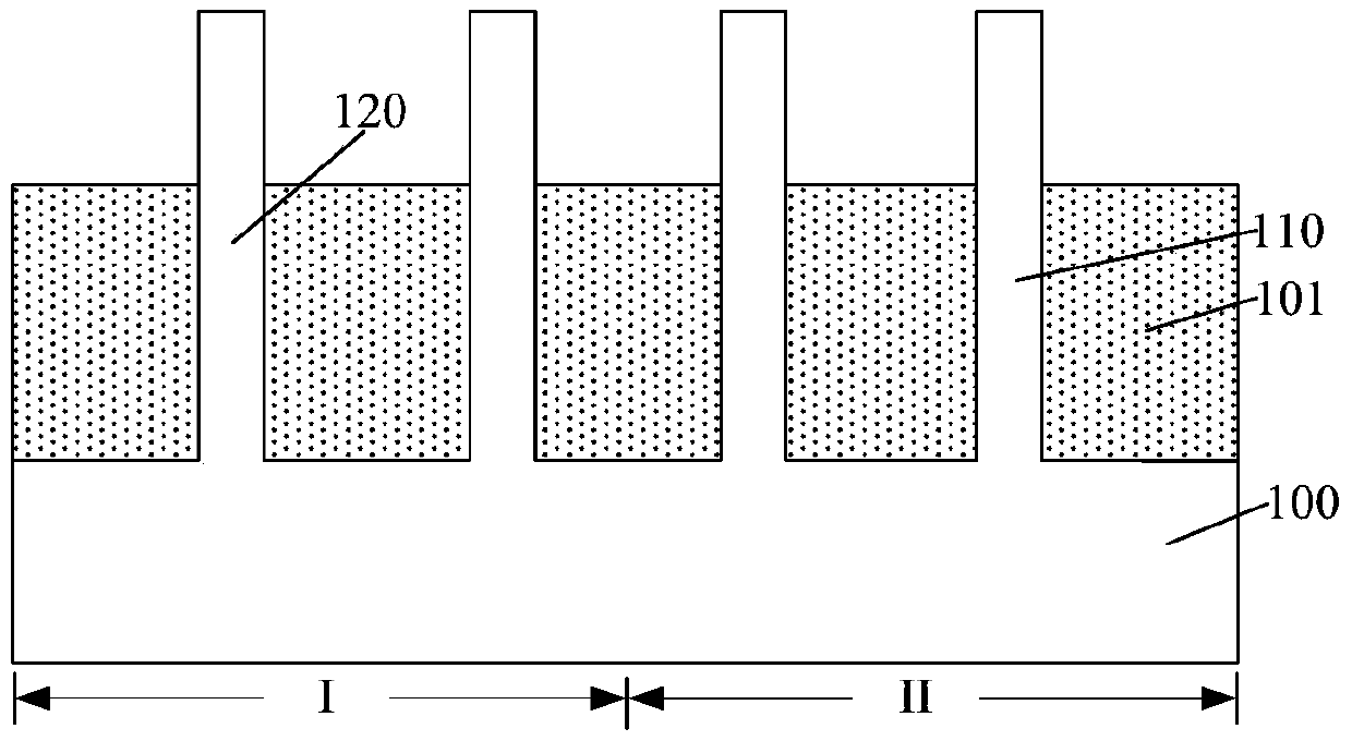
[0015] A base is provided, the base includes a substrate and a fin protruding from the substrate, the substrate includes an N-type region and a P-type region; forming a part of the side across the fin and covering the fin A dummy gate structure on the wall surface and a top surface; a source-drain doped region is formed in the fins on both sides of the dummy gate structure; a bottom interlayer dielectric layer is formed on the substrate between the fins, and the bottom interlayer The top of the dielectric layer is flush with the top of the dummy gate structure; the dummy gate structure is removed, a first opening is formed in the interlayer dielectric layer at the bottom of the N-type region, and a first open...


PUM


Abstract

The invention discloses a semiconductor structure and a forming method therefor, and the method comprises the steps: providing a substrate; forming metal gate structures on the substrate on the substrate, wherein each metal gate structure comprise a gate dielectric layer, a work function layer located on the gate dielectric layer, and a metal layer located on the work function layer; forming a barrier layer at the tops of the metal gate structures; forming an interlayer dielectric layer on the substrate between the metal gate structures; forming a contact hole plug passing through the interlayer dielectric layer; and carrying out the annealing treatment of the substrate after the forming of the contact hole plug. After the forming of the metal gate structures, the barrier layer is formed at the tops of the metal gate structures. The barrier layer is used for protecting the metal gate structures in the subsequent annealing treatment, and prevents the atoms liable to diffuse in the annealing treatment to diffuse to the work function layers of the metal gate structures, thereby avoiding the impact on the work function values of the work function layers, and achieving optimization of the electrical performances of a semiconductor device.

Description

technical field [0001] The invention relates to the field of semiconductors, in particular to a semiconductor structure and a forming method thereof. Background technique [0002] The main semiconductor device of an integrated circuit, especially a very large scale integrated circuit, is a metal-oxide-semiconductor field effect transistor (MOS transistor). With the continuous development of integrated circuit manufacturing technology, the technology nodes of semiconductor devices continue to decrease, and the geometric dimensions of semiconductor devices follow Moore's law. When the size of semiconductor devices is reduced to a certain extent, various secondary effects caused by the physical limits of semiconductor devices appear one after another, and it becomes more and more difficult to scale down the feature size of semiconductor devices. Among them, in the field of semiconductor manufacturing, the most challenging thing is how to solve the problem of large leakage curr...

Claims


Application Information

Patent Timeline
Patent Type & Authority Patents(China)
IPC IPC(8): H01L21/8238H01L27/092H01L29/78
Inventor 周飞
Owner SEMICON MFG INT (SHANGHAI) CORP
Why Eureka
Try Eureka