Laminated film and preparation method thereof

A thin film and lamination technology, applied in the field of solar cell manufacturing, can solve problems such as film peeling off and affect production quality, and achieve the effect of avoiding peeling off and improving production quality.

Inactive Publication Date: 2018-05-15
LINGFAN RENEWABLE ENERGY TECH BEIJING CO LTD
View PDF6 Cites 4 Cited by
  • Summary
  • Abstract
  • Description
  • Claims
  • Application Information

AI Technical Summary

Problems solved by technology

In the prior art, after the metal film layer is formed, the inherent stress state causes strain at the interface between the meta

Method used


Image

  • Laminated film and preparation method thereof
  • Laminated film and preparation method thereof

Examples


preparation example Construction

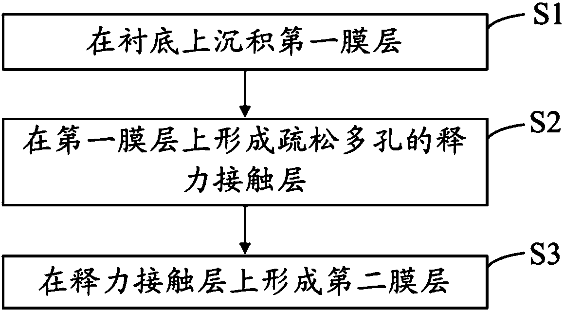
[0027] Such as figure 1 As shown, the embodiment of the present invention provides a method for preparing a laminated film, comprising the following steps:

[0028] S1. Depositing a first film layer on a substrate;

[0029] S2, forming a loose and porous force-releasing contact layer on the first film layer;

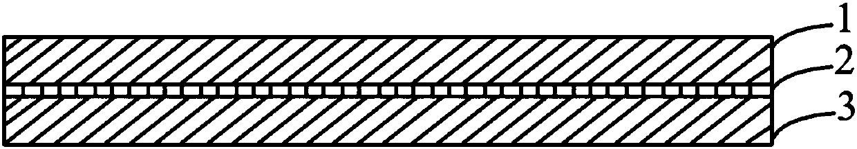
[0030] S3. Form a second film layer on the force-releasing contact layer, wherein: the first film layer is a metal layer, and the second film layer is a semiconductor layer, or the first film layer is a semiconductor layer, and the second film layer is a metal layer.

[0031] In the above steps, a metal layer may be deposited on the substrate first, and a semiconductor layer may be formed on the release contact layer; or a semiconductor layer may be deposited on the substrate first, and correspondingly, a metal layer may be formed on the release contact layer.

[0032] The preparation method of the laminated film provided by the embodiment of the present invention depo...


PUM


Abstract

The invention provides a laminated film and a preparation method thereof. The preparation method comprises the following steps that: a first film layer is deposited on a substrate, wherein the first film layer can be a metal layer or a semiconductor layer; a loose and porous force-release contact layer is formed on the first film layer; and a second film layer is formed on the force-release contact layer, wherein the second film layer can be a semiconductor layer or a metal layer. According to the laminated film and the preparation method thereof provided by the invention, the force-release contact layer is deposited, so that stress between the metal layer and the semiconductor layer can be released, the film layers can be prevented from falling off, and production quality is improved.

Description

technical field [0001] The invention relates to the manufacturing technology of solar cells, in particular to a method for preparing a laminated film and the laminated film. Background technique [0002] In the current semiconductor device manufacturing fields such as photovoltaics and flat panel displays, in order to meet the multiple needs of products, magnetron sputtering thin film technology is widely used in the preparation of complex devices with specific functions. Therefore, in the actual process, it is necessary to laminate two or more layers of different materials and different functions. Among them, the structure of metal and semiconductor laminated films is widely used as the electrode structure of the front and back contacts. [0003] There are significant differences in mechanical and electrical properties between metals and semiconductor materials. When they are in contact with each other in the form of a film to form an interface, serious physical property mi...

Claims


Application Information

Patent Timeline
IPC IPC(8): H01L21/02C23C14/00C23C14/08C23C14/16C23C14/34
CPCC23C14/0036C23C14/08C23C14/165C23C14/34H01L21/02502C23C14/0057C23C14/024C23C14/025C23C14/3492C23C28/322C23C28/34H01L31/022425
Inventor 田晶曲铭浩胡超黄昭雄吴建清徐国军
Owner LINGFAN RENEWABLE ENERGY TECH BEIJING CO LTD
Why Eureka
Try Eureka