Optical reference point recognition method and system, computer readable storage medium and equipment

A recognition method and fiducial point technology, applied in computing, special data processing applications, instruments, etc., can solve problems such as the inability to automatically identify and define optical fiducial points, and achieve the effect of reducing manual steps

Active Publication Date: 2018-05-18
VAYO SHANGHAI TECH
View PDF9 Cites 7 Cited by
  • Summary
  • Abstract
  • Description
  • Claims
  • Application Information

AI Technical Summary

Problems solved by technology

[0007] In view of the shortcomings of the prior art described above, the object of the present invention is to provide an optical fiducial point identification method, sys

Method used


Image

  • Optical reference point recognition method and system, computer readable storage medium and equipment
  • Optical reference point recognition method and system, computer readable storage medium and equipment
  • Optical reference point recognition method and system, computer readable storage medium and equipment

Examples


Embodiment 1

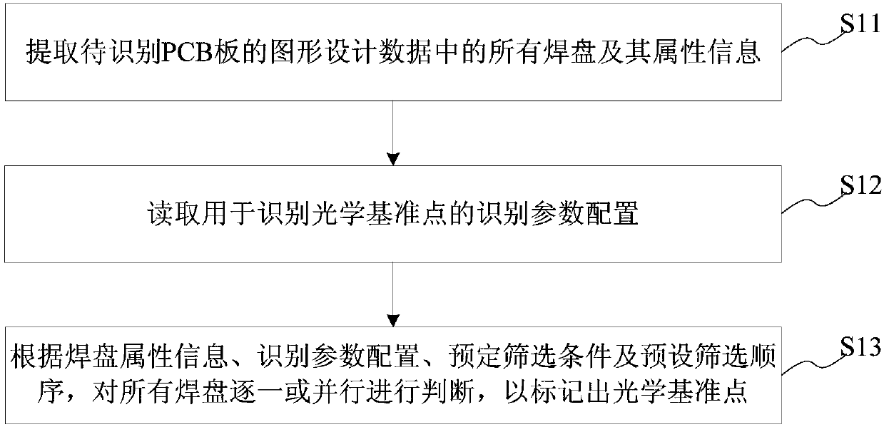
[0033] This embodiment provides an optical fiducial point recognition method, including:

[0034] Extract all pads and their attribute information in the graphic design data of the PCB board to be identified;

[0035] Read the identification parameter configuration used to identify the optical reference point;

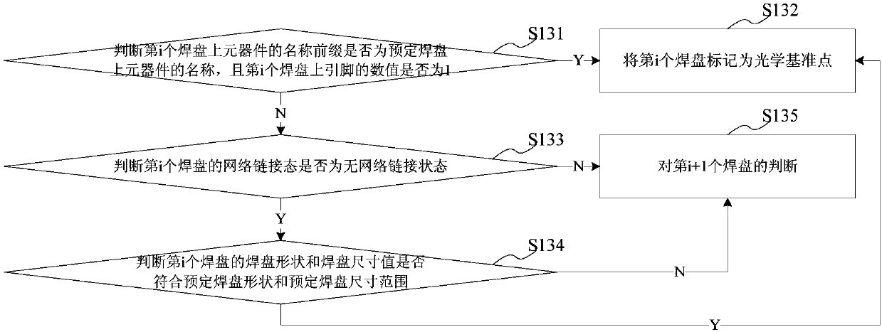
[0036] All pads are judged one by one or in parallel according to the pad attribute information, identification parameter configuration, predetermined screening conditions and a preset screening sequence combined with the predetermined screening conditions, so as to mark the optical reference point.

[0037] The optical fiducial point recognition method provided by this embodiment will be described in detail below with reference to the figures. The optical fiducial point recognition method described in this embodiment is applied to the graphic data of the PCB board. see Figure 1A , is shown as a schematic flowchart of an optical fiducial point recognition method in ...

Embodiment 2

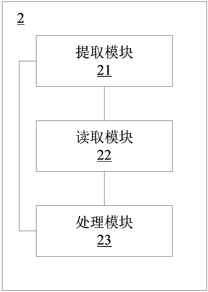
[0076] This embodiment provides an optical fiducial point recognition system, including:

[0077] An extraction module, configured to extract all pads and their attribute information in the graphic design data of the PCB board to be identified;

[0078] A reading module, configured to read the identification parameter configuration used to identify the optical reference point;

[0079] The processing module is configured to judge all pads one by one or in parallel according to the pad attribute information, identification parameter configuration, predetermined screening conditions and a preset screening order combined with the predetermined screening conditions, so as to mark optical reference points.

[0080] The optical fiducial point recognition system provided by this embodiment will be described in detail below with reference to the figures. It should be noted that it should be understood that the above division of each module of the optical fiducial point recognition sy...

Embodiment 3

[0101] This embodiment provides a device, which includes: a processor, a memory, a transceiver, a communication interface, and a system bus; the memory and the communication interface are connected to the processor and the transceiver through the system bus and complete mutual communication, and the memory is used for The computer program is stored, the communication interface is used to communicate with other devices, the processor and the transceiver are used to run the computer program, so that the device executes the steps of the above optical reference point identification method.

[0102] The system bus mentioned above may be a Peripheral Component Interconnect (PCI for short) bus or an Extended Industry Standard Architecture (EISA for short) bus or the like. The system bus can be divided into address bus, data bus, control bus and so on. The communication interface is used to realize the communication between the database access device and other devices (such as client,...


PUM


Abstract

The invention provides an optical reference point recognition method and system, a computer readable medium and equipment. The optical reference point recognition method comprises the steps of recognizing all pads and pad attribution information in graphic design data of a PCB to be recognized; reading recognition parameter configuration used for recognizing an optical reference point; according to the pad attribution information, the recognition parameter configuration and predetermined screening conditions in combination with a preset screening sequence of the predetermined screening conditions, judging all the pads one to one or parallelly to mark the optical reference point. The optical reference point for prejudgment can be provided for a client for reference, the client does not needto watch the board to manually look for the optical reference point by himself/herself, thus the steps of artificial participation in the SMT manufacturing procedure can be reduced, a key problem inautomated program manufacturing is solved, and technical support is provided for intelligent manufacturing in the electronic industry.

Description

technical field [0001] The invention belongs to the technical field of detection of PCB circuit boards, and relates to an identification method and system, in particular to an optical reference point identification method, system, computer-readable storage medium and equipment. Background technique [0002] Two or more optical reference points are designed on the PCB circuit board. The purpose is to locate the entire PCB board and facilitate the position identification of SMT equipment. Almost all SMT equipment such as screen printing machines, placement machines, optical inspection machines, etc. This benchmark will be used. [0003] At present, most of the procedures for making SMT equipment in the industry are manually moved to the position of the PCB optical reference point to find it; or engineers read the graphics in the design file through software and then designate this point as the optical reference point according to their own work experience. [0004] Intelligen...

Claims


Application Information

Patent Timeline
IPC IPC(8): G06F17/50
CPCG06F30/398
Inventor 钱胜杰刘继硕刘丰收
Owner VAYO SHANGHAI TECH
Why Eureka
Try Eureka