A kind of anti-dual-node flipping latch

A dual-node inversion and latch technology, which is applied in the fields of reliability improvement of field effect transistors, logic circuit coupling/interface using field effect transistors, reliability improvement modification, etc., can solve the problem that the latch cannot resist dual-node inversion, Low area overhead, etc.

Active Publication Date: 2021-07-13
INST OF MICROELECTRONICS CHINESE ACAD OF SCI
View PDF7 Cites 0 Cited by
  • Summary
  • Abstract
  • Description
  • Claims
  • Application Information

AI Technical Summary

Problems solved by technology

[0005] The embodiment of the present application solves the technical problem that the latch in the prior art cannot realize anti-double-node flipping in a small-area circuit structure by providing a latch that resists double-node flipping, so that the latch provided by the present application The device achieves the technical effects of improving the ability of digital integrated circuits to resist single event flipping under harsh conditions, resisting double-node flipping, high reliability, and low area overhead

Method used


Image

  • A kind of anti-dual-node flipping latch
  • A kind of anti-dual-node flipping latch
  • A kind of anti-dual-node flipping latch

Examples


Embodiment 1

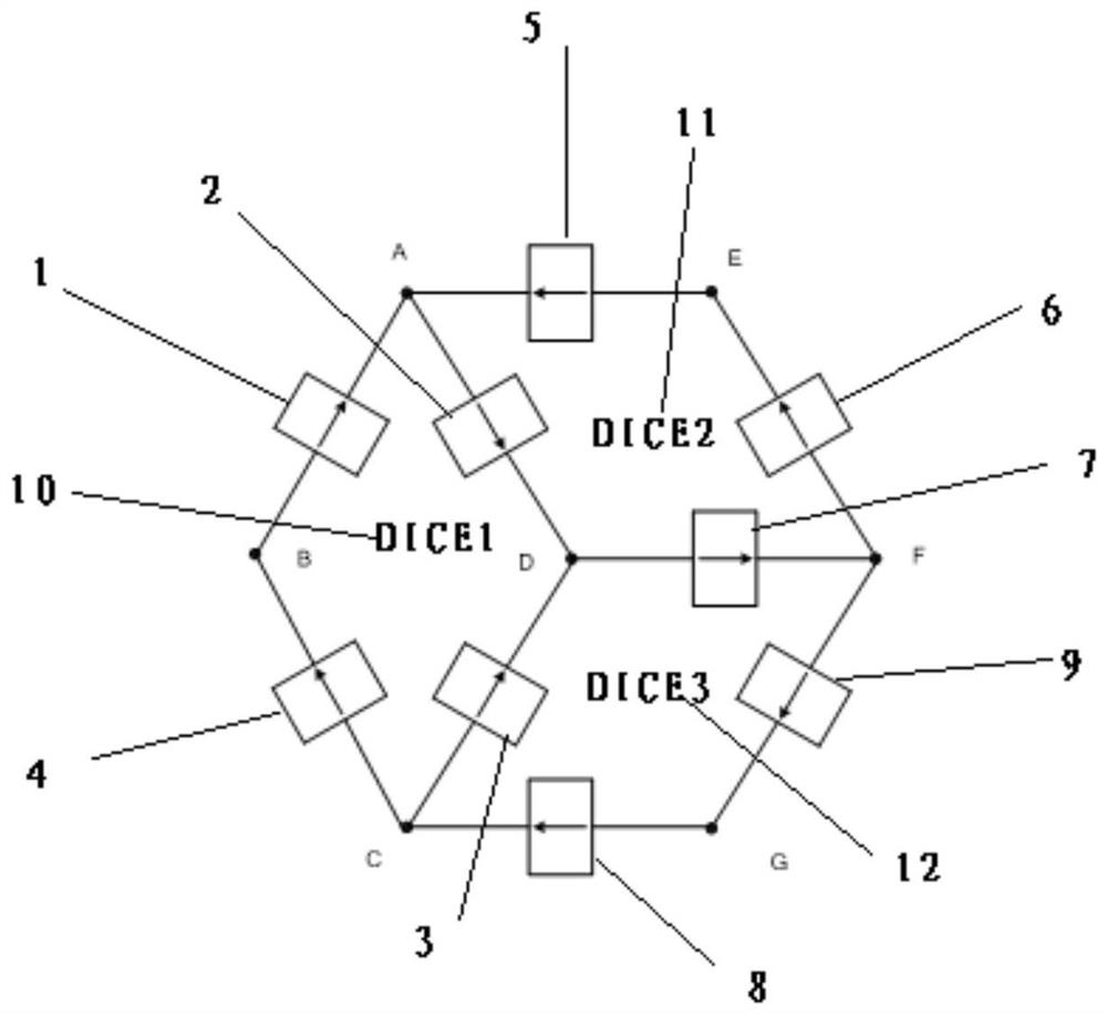
[0027] figure 1 It is a schematic structural diagram of a latch resistant to double-node flipping provided by the embodiment of the present application. Such as figure 1 shown, the latch consists of:

[0028] The latch has a storage node A, a storage node B, a storage node C, a storage node D, a storage node E, a storage node F, and a storage node G;

[0029] Specifically, a latch (Latch) is a memory unit circuit sensitive to a pulse level, and they can change states under the action of a specific input pulse level. Latch is to temporarily store the signal to maintain a certain level state. The main function of the latch is to cache, secondly to complete the asynchronous problem between the high-speed controller and the slow peripheral, then to solve the problem of the driver, and finally to solve the problem that an I / O port can output and input question. A latch is an input that uses level control data, and it includes a latch without enable control and a latch with ena...

Embodiment 2

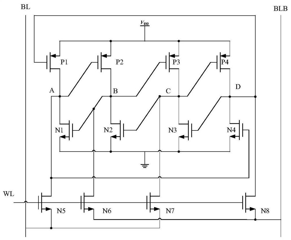
[0038] In order to further explain the anti-double-node flipping latch provided in the present application, the embodiment of the present application describes the working principle of the anti-double-node flipping latch.

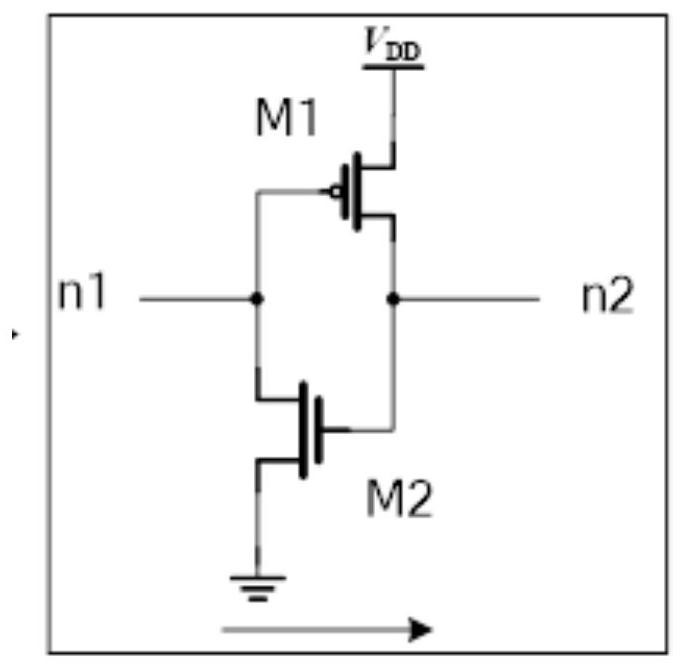
[0039] When the latch is in conduction mode, as Figure 4 As shown, the input data In are transmitted to storage node A, storage node C and storage node F through CMOS transmission gates TG1, TG2 and TG3 respectively, while storage node B, storage node D, storage node E and storage node G are connected with the input data In is logically the opposite. D is output to the output node Q through a clocked inverter, so the input In is logically the same as the output Q. In holdover mode, these redundant nodes have the ability to restore the correct logic. As a result, when the dual-node flip occurs, it can be restored to the normal logic level by the remaining storage nodes, which improves the ability of digital integrated circuits to resist single-event flipp...


PUM


Abstract

An embodiment of the present application provides an anti-dual-node inversion latch, which relates to the technical field of integrated circuits. The latch includes: the latch has a storage node A, a storage node B, a storage node C, and a storage node D. Storage node E, storage node F, storage node G; the latch further has: a first cross-coupling structure; a second cross-coupling structure; a third cross-coupling structure; a fourth cross-coupling structure; a fifth cross-coupling structure structure; sixth cross-coupling structure; seventh cross-coupling structure; eighth cross-coupling structure; ninth cross-coupling structure. The technical problem that the latch in the prior art cannot achieve anti-double-node inversion in a small-area circuit structure is solved, so that the latch provided by the present application can improve the ability of the digital integrated circuit to resist single-event inversion under harsh conditions. , The technical effect of anti-dual node flipping, high reliability and low area overhead.

Description

technical field [0001] The invention relates to the technical field of integrated circuits, in particular to a double-node flip-resistant latch. Background technique [0002] A latch (Latch) is a memory cell circuit that is sensitive to pulse levels, and they can change states under the action of a specific input pulse level. Latch is to temporarily store the signal to maintain a certain level state. One of the functions of the latch is to solve the problem that an I / O port can both output and input. [0003] However, in the process of realizing the technical solution of the invention in the embodiment of the present application, the inventor of the present application found that the above-mentioned technology has at least the following technical problems: [0004] The latches in the prior art cannot realize anti-double-node flipping in a small-area circuit structure. Contents of the invention [0005] The embodiment of the present application solves the technical probl...

Claims


Application Information

Patent Timeline
Patent Type & Authority Patents(China)
IPC IPC(8): H03K19/003H03K19/0185
CPCH03K19/00315H03K19/018507
Inventor 刘梦新刘海南赵发展卜建辉罗家俊韩郑生
Owner INST OF MICROELECTRONICS CHINESE ACAD OF SCI
Why Eureka
Try Eureka