Two-sided laser processing method for PCB array micropores

A laser processing method and micro-hole technology, applied in laser welding equipment, metal processing equipment, manufacturing tools, etc., can solve the problems of reducing production efficiency and increasing material costs, and achieve heat dissipation, heat-free processing, and processing high precision effect

Active Publication Date: 2018-06-01
GUANGDONG UNIV OF TECH
View PDF7 Cites 13 Cited by
  • Summary
  • Abstract
  • Description
  • Claims
  • Application Information

AI Technical Summary

Problems solved by technology

Patent CN201210475417.4 discloses a circuit board drilling method (including laser drilling and mechanical drilling process), which can well avoid problems such as hole deformation caused by thermal influence, but this method needs to set up functional areas and test Area, test and adjust parameters in the test area first, and then process in the functional area, which increases the cost of materials on the one hand, and reduces production efficiency on the other hand

Method used


Image

  • Two-sided laser processing method for PCB array micropores
  • Two-sided laser processing method for PCB array micropores
  • Two-sided laser processing method for PCB array micropores

Examples


Embodiment 1

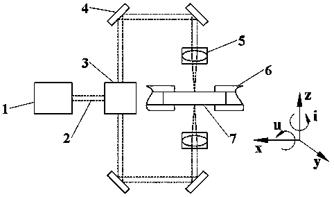
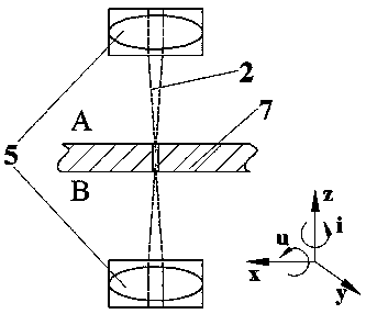
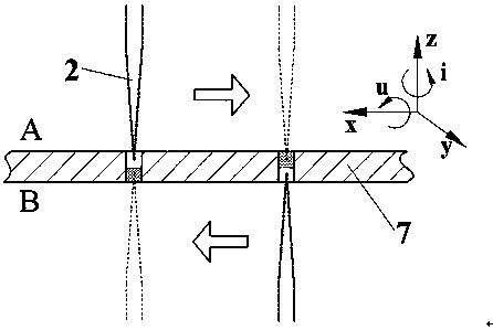
[0029] like figure 1 and 2 As shown, the present embodiment provides a double-sided laser processing method for PCB7 array microholes, and measures the ablation threshold value of the required processing layer material of PCB7; the processed PCB7 is fixed on the ultra-precision platform 6 and the ultra-precision The precision platform 6 rotates along the u direction; the laser 1 outputs the laser beam 2, which is divided into two laser beams 2 by the beam splitting module 3, and the two laser beams 2 respectively pass through the mirror 4 and pass through the focusing module 5, and are installed on the ultra-precision platform The front and back sides of PCB7 of 6 are processed.

[0030] A and B sides are PCB7 with symmetrical structure and through-hole processing with a depth-to-diameter ratio of more than 2:1: the laser system outputs two laser beams 2 as A and B, the output wavelength is 355nm, the pulse width is 80ns, and the power is 8W , a laser beam 2 with a repetitio...


PUM

PropertyMeasurementUnit
wavelengthaaaaaaaaaa

Abstract

The invention provides a two-sided laser processing method for PCB array micropores. The two-sided laser processing method comprises the following steps that S1, ablation threshold values of all material layers, needing to be processed, of a PCB are tested; S2, the PCB is fixed to an ultra-precise platform, and the rotation angle of the ultra-precise platform in the u direction is set; and S3, a laser beam is emitted by a laser device and divided into two beams by a laser dividing module, and then, the laser beams pass through a reflecting mirror and a focusing module in sequence so that the front face and the back face of the PCB clamped to the ultra-precise platform can be subjected to laser micropore processing correspondingly. The two-sided laser processing method has the advantages ofbeing high in efficiency and precision, low in cost and the like.

Description

technical field [0001] The invention relates to PCB processing, in particular to a double-sided laser processing method for PCB array microholes. Background technique [0002] With the development of information technology, PCB (Printed Circuit Board, printed circuit board) is developing towards the trend of miniaturization, light weight and high density, which puts higher requirements on the microhole processing of PCB. In the traditional PCB drilling process, mechanical drilling is most commonly used. With the continuous reduction of PCB aperture requirements, the traditional mechanical drilling method has disadvantages such as easy needle breakage, low drill strength, and low rigidity, and is not suitable for microhole processing with apertures <100 μm. [0003] Laser is a high-energy beam processing method that does not contact the workpiece. Due to the high absorption efficiency of resin and other materials for specific wavelength lasers, laser is especially suitabl...

Claims


Application Information

Patent Timeline
Patent Type & Authority Applications(China)
IPC IPC(8): B23K26/36B23K26/60B23K26/067B23K26/08
CPCB23K26/0676B23K26/0861B23K26/36B23K26/60
Inventor 王成勇唐梓敏郑李娟王宏建黄欣杜策之胡小月
Owner GUANGDONG UNIV OF TECH
Why Eureka
Try Eureka