Reading method and device of memory unit

A technology for storing cells and reading voltage, applied in the field of memory, can solve problems such as large changes in current, increased reading difficulty, and increased design complexity of current comparators

Inactive Publication Date: 2018-06-01
GIGADEVICE SEMICON (BEIJING) INC
View PDF8 Cites 5 Cited by
  • Summary
  • Abstract
  • Description
  • Claims
  • Application Information

AI Technical Summary

Problems solved by technology

The existing memory cell reading method is to apply a fixed read voltage to the memory cell, but due to the characteristics of the memory chip itself, when the temperature of the memory chip is higher than a certain value or lower than a certain value, the threshold voltage of the memory cell will change , if the read voltage is constant, the change of the threshold volta...

Method used


Image

  • Reading method and device of memory unit
  • Reading method and device of memory unit
  • Reading method and device of memory unit

Examples


Embodiment 1

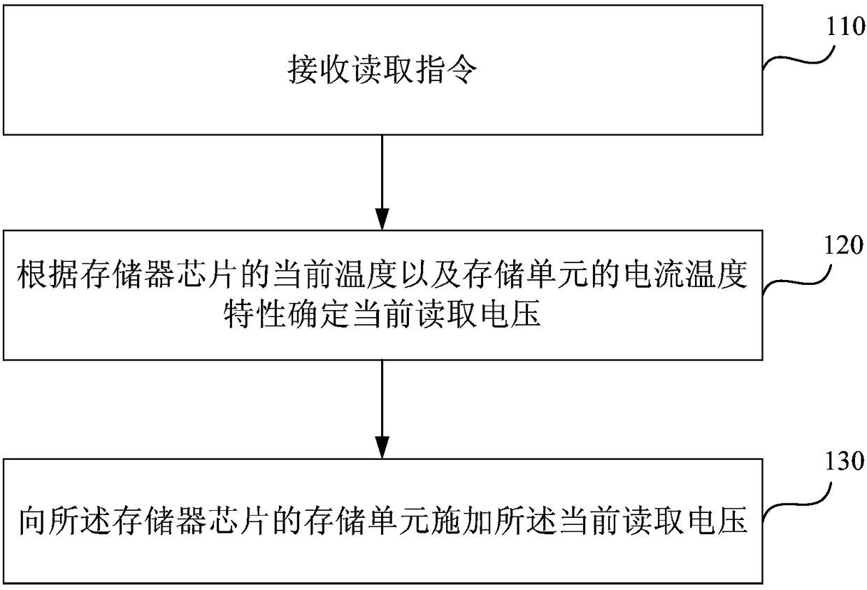
[0045] figure 2 It is a flow chart of a method for reading a storage unit provided by Embodiment 1 of the present invention. This embodiment is applicable to the case of performing a reading operation on a storage unit of a memory chip when the temperature of the memory chip often changes. see figure 2 The method for reading the storage unit provided in this embodiment specifically includes the following steps:

[0046] Step 110, receiving a read instruction.

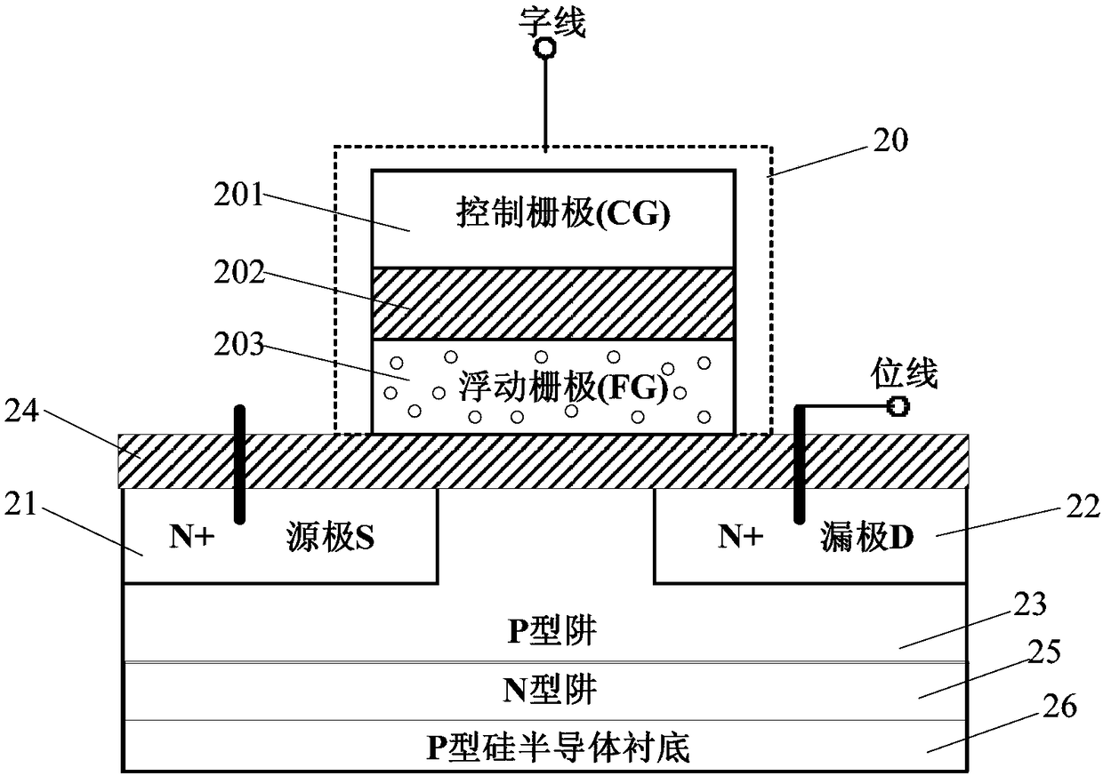
[0047] By writing program codes, the flash memory can be controlled to perform three major operations, namely, read operation, write operation (that is, programming operation) and erase operation; among them, the principle of read operation is to apply a read operation to the gate of the storage unit. Voltage, at this time, a current will be generated in the memory cell, compare this current with the reference current, and finally obtain whether the current state of the memory cell is an erased state or a programmed...

Embodiment 2

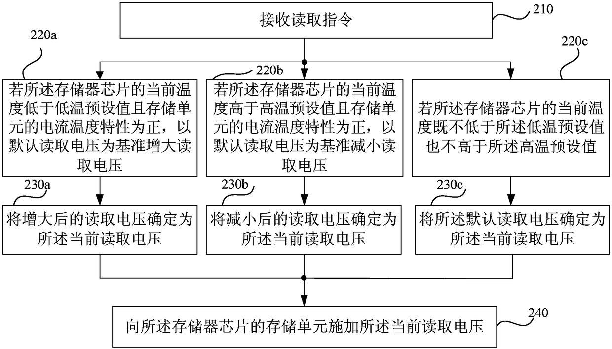
[0057] image 3 It is a flow chart of a method for reading a storage unit provided by Embodiment 2 of the present invention. This embodiment is further optimized on the basis of Embodiment 1. The advantage of optimization is that when the temperature of the memory chip is higher than the high temperature preset value Or when the temperature is lower than the low temperature preset value, a reading voltage matching the temperature is determined to ensure reading performance. Typically, this embodiment takes a memory cell with a positive temperature characteristic as an example, that is, when the same read voltage is applied, the current flowing through the memory cell increases as the temperature increases and decreases as the temperature decreases. For details, please refer to image 3 , the method specifically includes the following steps:

[0058] 210. Receive a read instruction.

[0059] 220a. If the current temperature of the memory chip is lower than the low temperatur...

Embodiment 3

[0075] Figure 4 It is a schematic structural diagram of a reading device for a storage unit provided in Embodiment 3 of the present invention, and the device specifically includes:

[0076] receiving module 310, determining module 320 and applying module 330;

[0077] Wherein, the receiving module 310 is used to receive the read instruction; the determination module 320 is used to determine the current read voltage according to the current temperature of the memory chip and the current temperature characteristics of the storage unit; the application module 330 is used to apply to the memory chip The memory cell applies the current read voltage.

[0078] Further, the device may further include: a detection module, configured to detect the current temperature of the memory chip through a temperature sensor before determining the current read voltage according to the current temperature of the memory chip and the current-temperature characteristic of the storage unit.

[0079]...


PUM


Abstract

The invention discloses a reading method and device of a memory unit. The method comprises the steps as follows: receiving a reading instruction; determining the current reading voltage according to the current temperature of a memory chip and the current temperature characteristic of the memory unit; applying the current reading voltage to the memory unit of the memory chip. According to the reading method of the memory unit, the current reading voltage is determined according to the current temperature of the memory chip and the current temperature characteristic of the memory unit and applied to the memory unit of the memory chip, so that the current variation of the memory unit is reduced by changing the reading voltage, and the reading performance of the memory unit is improved.

Description

technical field [0001] The present invention relates to the technical field of memory, in particular to a method and device for reading a memory unit. Background technique [0002] Flash memory (flash memory) is a kind of non-volatile memory (Non-volatile memory), which uses a nonlinear macro-cell mode inside, has the advantages of large capacity and fast rewriting speed, and is suitable for storing large amounts of data. [0003] In a flash memory, a memory cell can be regarded as a metal-oxide-semiconductor field-effect transistor (Metal-Oxide-Semiconductor Field-Effect Transistor, MOSFET). figure 1 It is a common MOSFET structure diagram, including a gate 20 , a source 21 , a drain 22 , a P-type silicon semiconductor substrate 23 , and a tunnel oxide layer 24 . The connection between them is as follows: P-type silicon semiconductor substrate 23 diffuses two N-type regions, and a layer of tunneling oxide layer 24 is covered on the top of P-type silicon semiconductor subst...

Claims


Application Information

Patent Timeline
IPC IPC(8): G11C7/04G11C16/26G11C16/30
CPCG11C7/04G11C16/26G11C16/30
Inventor 张建军胡洪
Owner GIGADEVICE SEMICON (BEIJING) INC
Why Eureka
Try Eureka