Electric potential control rapid transverse insulated gate bipolar transistor
A technology of bipolar transistors and insulated gates, applied in circuits, electrical components, semiconductor devices, etc., can solve problems such as the difficulty of further optimization of the relationship between off-time and on-voltage drop constraints, work reliability problems, etc., and achieve the suppression of NDR phenomenon, improving job stability, and optimizing the effect of trade-off relations
- Summary
- Abstract
- Description
- Claims
- Application Information
AI Technical Summary
Problems solved by technology
Method used
Image

Examples
Embodiment 1
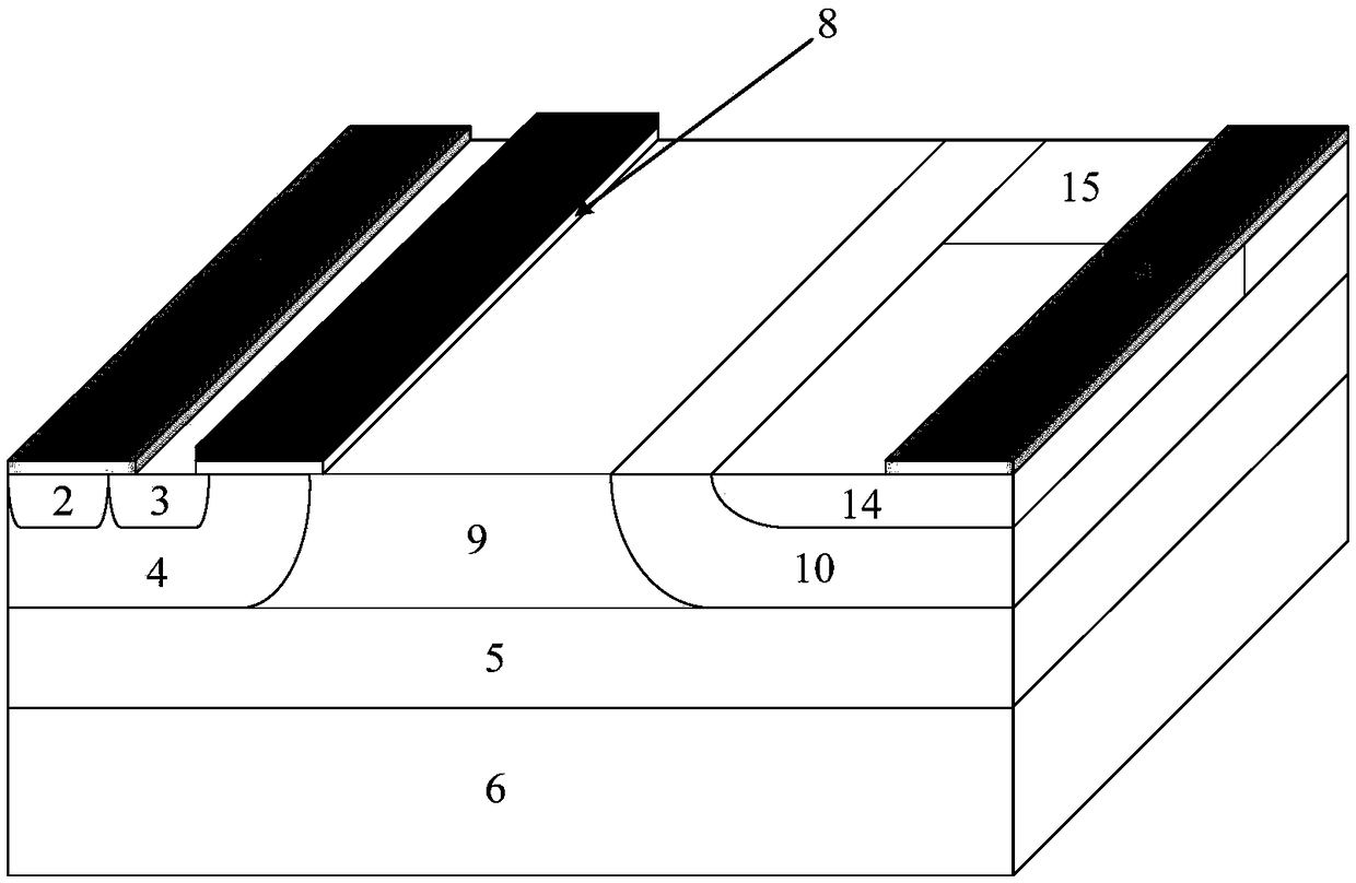
[0042] Such as Figure 4 As shown, a potential-controlled fast lateral insulated gate bipolar transistor includes an SOI substrate, a drift region, an anode region, a cathode region and a gate region, and is characterized in that: the SOI substrate includes a buried oxide layer 5, a lining Bottom 6 and top silicon layer.
[0043] The buried oxide layer 5 covers the substrate layer 6 .
[0044] The top silicon layer is located on the buried oxide layer 5 .
[0045] A conductive functional region of a potential controlled fast lateral insulated gate bipolar transistor is formed in the top silicon layer.
[0046] The drift region is attached above the buried oxide layer 5 , and the drift region is composed of an N-base region 9 .
[0047] The anode region and the cathode region are respectively located on two sides of the N base region 9 .
[0048] The gate area is attached above the cathode area.
[0049] The substrate layer 6 is made of P-type or N-type silicon material, a...
Embodiment 2
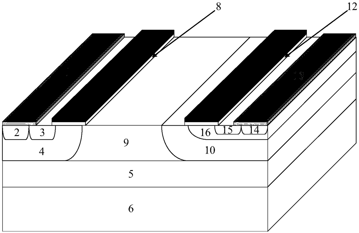
[0067] A potential-controlled fast lateral insulated gate bipolar transistor, comprising an SOI substrate, a drift region, an anode region, a cathode region and a gate region, characterized in that the SOI substrate includes a buried oxide layer 5, a substrate layer 6 and top silicon layer.
[0068] The buried oxide layer 5 covers the substrate layer 6 .
[0069] The top silicon layer is located on the buried oxide layer 5 .
[0070] A conductive functional region of a potential controlled fast lateral insulated gate bipolar transistor is formed in the top silicon layer.
[0071] The drift region is attached above the buried oxide layer 5 , and the drift region is composed of an N-base region 9 .
[0072] The anode region and the cathode region are respectively located on two sides of the N base region 9 .
[0073] The gate area is attached above the cathode area.
[0074] The substrate layer 6 is made of P-type or N-type silicon material, and its typical impurity concentr...
PUM
| Property | Measurement | Unit |
|---|---|---|
| Thickness | aaaaa | aaaaa |
Abstract
Description
Claims
Application Information
 - Generate Ideas
- Intellectual Property
- Life Sciences
- Materials
- Tech Scout
- Unparalleled Data Quality
- Higher Quality Content
- 60% Fewer Hallucinations
Browse by: Latest US Patents, China's latest patents, Technical Efficacy Thesaurus, Application Domain, Technology Topic, Popular Technical Reports.
© 2025 PatSnap. All rights reserved.Legal|Privacy policy|Modern Slavery Act Transparency Statement|Sitemap|About US| Contact US: help@patsnap.com