Heterojunction potential controlled insulated grid bipolar transistor
A technology of bipolar transistors and heterojunctions, applied in circuits, electrical components, semiconductor devices, etc., to achieve the effects of improving work stability, optimizing tradeoffs, and suppressing NDR phenomena
- Summary
- Abstract
- Description
- Claims
- Application Information
AI Technical Summary
Problems solved by technology
Method used
Image

Examples
Embodiment 1
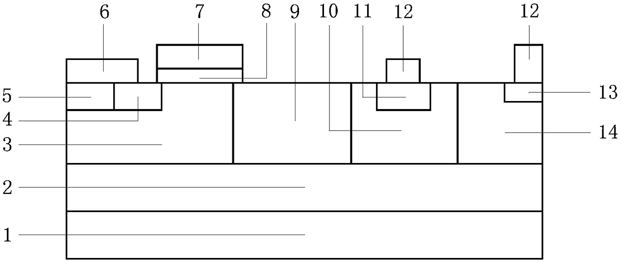
[0041] like figure 1 As shown, a heterojunction potential-controlled insulated gate bipolar transistor is characterized in that it includes an SOI substrate, a drift region, an anode region, a cathode region and a gate region.
[0042] The SOI substrate includes a substrate layer 1, a dielectric layer 2 and a top layer of silicon.
[0043] The substrate layer 1 is a P-type or N-type doped silicon material; its typical impurity concentration is the 14th power;
[0044] The dielectric layer 2 covers the substrate layer 1, and the dielectric layer 2 is made of silicon dioxide. The typical thickness is 0.5μm to 5μm according to the withstand voltage requirements of the designed device.
[0045] The top layer silicon covers the dielectric layer 2, and the top layer silicon is a P-type or N-type doped silicon material.
[0046] The conductive functional region of a heterojunction potential controlled insulated gate bipolar transistor is formed in the top layer silicon.
[0047] ...
Embodiment 2
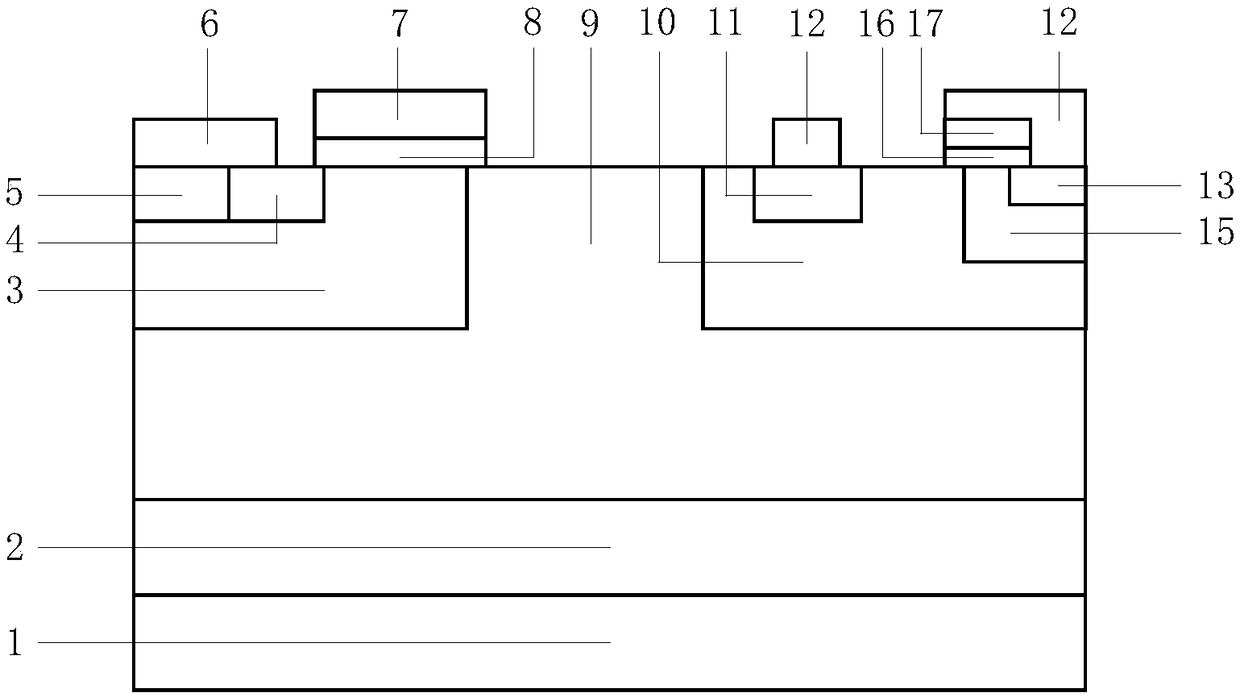
[0064] like figure 2 As shown, a heterojunction potential-controlled insulated gate bipolar transistor is characterized in that it includes an SOI substrate, a drift region, an anode region, a cathode region and a gate region.
[0065] The SOI substrate includes a substrate layer 1, a dielectric layer 2 and a top layer of silicon.
[0066] The substrate layer 1 is a P-type or N-type doped silicon material; its typical impurity concentration is the 14th power;
[0067] The dielectric layer 2 covers the substrate layer 1, and the dielectric layer 2 is made of silicon dioxide. The typical thickness is 0.5μm to 5μm according to the withstand voltage requirements of the designed device.
[0068] The top layer silicon covers the dielectric layer 2, and the top layer silicon is a P-type or N-type doped silicon material.
[0069] The conductive functional region of a heterojunction potential controlled insulated gate bipolar transistor is formed in the top layer silicon.
[0070]...
Embodiment 3
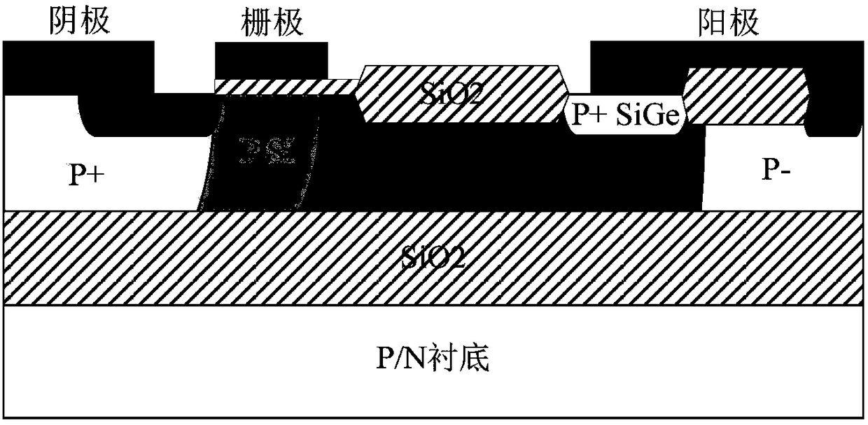
[0087] like image 3 As shown, a heterojunction potential-controlled insulated gate bipolar transistor is characterized in that it includes an SOI substrate, a drift region, an anode region, a cathode region and a gate region.
[0088] The SOI substrate includes a substrate layer 1, a dielectric layer 2 and a top layer of silicon.
[0089] The substrate layer 1 is a P-type or N-type doped silicon material; its typical impurity concentration is the 14th power;
[0090] The dielectric layer 2 covers the substrate layer 1, and the dielectric layer 2 is made of silicon dioxide. The typical thickness is 0.5μm to 5μm according to the withstand voltage requirements of the designed device.
[0091] The top layer silicon covers the dielectric layer 2, and the top layer silicon is a P-type or N-type doped silicon material.
[0092] The conductive functional region of a heterojunction potential controlled insulated gate bipolar transistor is formed in the top layer silicon.
[0093] ...
PUM
 Abstract
Description
Claims
Application Information
 - Generate Ideas
- Intellectual Property
- Life Sciences
- Materials
- Tech Scout
- Unparalleled Data Quality
- Higher Quality Content
- 60% Fewer Hallucinations
Browse by: Latest US Patents, China's latest patents, Technical Efficacy Thesaurus, Application Domain, Technology Topic, Popular Technical Reports.
© 2025 PatSnap. All rights reserved.Legal|Privacy policy|Modern Slavery Act Transparency Statement|Sitemap|About US| Contact US: help@patsnap.com