Novel power semiconductor device

A technology of power semiconductors and devices, applied in the direction of semiconductor devices, electrical components, circuits, etc.

Inactive Publication Date: 2014-06-25
HANGZHOU ENNENG TECH
View PDF4 Cites 5 Cited by
  • Summary
  • Abstract
  • Description
  • Claims
  • Application Information

AI Technical Summary

Problems solved by technology

However, SA-LIGBT has a negative resistance phenomenon NDR (Negative Differential Resistance), which is caused by the sudden switching of the device between the two working modes of LDMOS and LIGBT

Method used


Image

  • Novel power semiconductor device
  • Novel power semiconductor device
  • Novel power semiconductor device

Examples


Embodiment 1

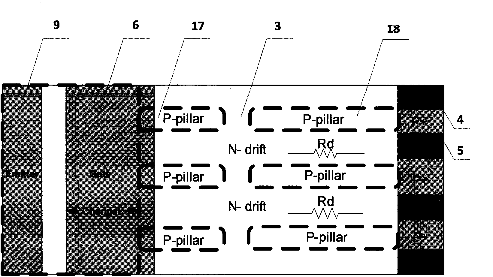
[0023] image 3 Shown is a top view structure diagram of a new type of power semiconductor device, including the anode P + Zone (5), anode N + Region (4), N-type drift region (3), emitter N + region (9), P-type channel region (6) and P-type pillar regions (17, 18).

[0024] The anode of the structure of the present invention adopts N + District (4) and P + In the overlapping short-circuit structure of the region (5), there are two parts of the P-type column region (17, 18) in the drift region, which are respectively connected with the P-type channel region (6) of the cathode and the P-type channel region (6) of the anode. + Area (5) is connected. Through the adjustment of these structures, the NDR phenomenon no longer occurs, the latch-up effect during high-current operation is effectively suppressed, the switching speed is greatly improved, and the withstand voltage of the device is also improved to a certain extent.

Embodiment 2

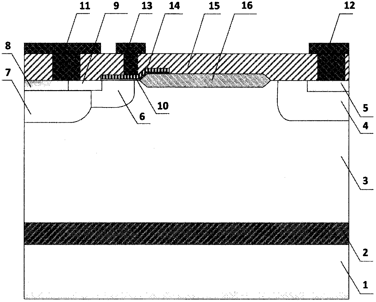
[0026] Figure 4 Shown is a new type of power semiconductor device along the anode N + Sectional drawing of the area. Including substrate (1), anode N + region (4), anode metal (12), N-type drift region (3), field oxide layer (16), cathode P + region (8), cathode P-type body region (7), P-type channel region (6), emitter N + region (9), cathode metal (11), polysilicon gate (14), LIGBT device gate oxide layer (10) and polysilicon gate metal (13).

[0027] When the device is just turned on, the anode N with P-type + \P + Fast SOI LIGBT device inversion channel formation with overlapping shorts. When a positive voltage is applied to the anode, the electron current in the inversion channel is injected into the drift region (3) and passes through the anode N + Area (4) is extracted, and the device works in LDMOS state at this time, and there is no conductance modulation phenomenon.

Embodiment 3

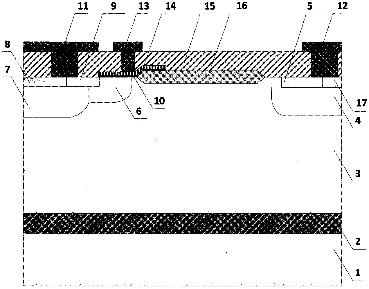
[0029] Figure 5 Shown is a new type of power semiconductor device along the anode P + Sectional drawing of the area. Including substrate (1), anode P + region (5), anode metal (12), N-type drift region (3), field oxide layer (16), cathode P + region (8), cathode P-type body region (7), P-type channel region (6), emitter N + region (9), cathode metal (11), polysilicon gate (14), LIGBT device gate oxide layer (10), polysilicon gate metal (13) and P-type pillar regions (17, 18).

[0030] Figure 5 and Figure 4 The difference is that it is more Figure 4 There are two more P-type pillar regions (17, 18), and its anode N + Zone (4) consists of anode P + District (5) replaces.

[0031] In order to make the NDR phenomenon of the anode short-circuit structure no longer occur, the resistance between the P-type pillars (4) should be large enough, so that a voltage difference of 0.7V can be reached when the current is extremely small, so that the anode P + (5) and the P-type pi...


PUM


Abstract

The invention relates to a semiconductor device, and discloses a novel power semiconductor device comprising a substrate (1), an anode P+ region (5), an anode N+ region (4), anode metal (12), an N-type drift region (3), a field oxide layer (16), a cathode P+ region (8), a cathode P-type body region (7), a P-type channel region (6), an emitting electrode N+ region (9), cathode metal (11), a poly-silicon gate (14), a gate oxide layer (10), poly-silicon gate metal (13) and P-type cylinder regions (17,18). The two P-type cylinder regions (17, 18) are additionally arranged in the P-type channel region (6) and the anode P+ region (5), and the structure that the anode P+ region (5) and the anode N+ region (4) are arranged in an alternating way is adopted so that the inverse resistance effect of the device is inhibited, the latch-up effect of the device in the high-current working state is overcome, turn-off speed and voltage resistance of the device are enhanced and power consumption of the device is reduced.

Description

technical field [0001] The invention relates to semiconductor power device technology. Background technique [0002] Lateral Insulated-Gate Bipolar Transistor LIGBT (Lateral Insulated-Gate Bipolar Transistor) is often used in the output stage of high-voltage power drive integrated circuits due to its low turn-on voltage drop and high input impedance to improve the lateral double-diffused metal oxide The contradiction between the withstand voltage and on-resistance of LDMOS (Lateral Double-diffused MOSFET) semiconductor field effect transistor. [0003] figure 1 The structural diagram of a traditional n-channel LIGBT device is given, in which, 1 is a P-type or N-type substrate, 2 is a buried oxide layer, 3 is an N-type drift region, and 4 is the same doping type as the N-type drift region 3 N-type buffer layer, 5 is the anode P+ region, 6 is the P-type channel region of the device, 7 is the P-type region with a higher concentration than the P-type channel region 6, and 8 is...

Claims


Application Information

Patent Timeline
Patent Type & Authority Applications(China)
IPC IPC(8): H01L29/739H01L29/06H01L29/417
CPCH01L29/7393H01L29/0615H01L29/0834
Inventor 何敏谢刚王柳敏王珏
Owner HANGZHOU ENNENG TECH
Why Eureka
Try Eureka