Collector-electrode short-circuit IGBT structure integrating diode

A collector short-circuit and diode technology, which is applied in the direction of circuits, transistors, electrical components, etc., can solve the problems of increasing the packaging area and cost of diodes and IGBTs

Inactive Publication Date: 2014-02-26
FOSHAN XINGUANG SEMICON
View PDF3 Cites 3 Cited by
  • Summary
  • Abstract
  • Description
  • Claims
  • Application Information

AI Technical Summary

Problems solved by technology

However, since the collector N + The existence of the region makes the device have a reverse resistance phenomenon. This is because the device is in the MOSFET working mode when it is just turned on. Only when the current reaches a certain value makes the collector P + District and N - When the PN junction voltage in the drift region reaches a voltage difference of 0.7V to form a forward bias, the device can enter the IGBT working mode, forming a conductance modulation effect
[0004] The application of traditional IGBT devices in many fields requires a diode to achieve current conversion during switching, which increases the packaging area and cost of diodes and IGBTs for production.

Method used


Image

  • Collector-electrode short-circuit IGBT structure integrating diode
  • Collector-electrode short-circuit IGBT structure integrating diode
  • Collector-electrode short-circuit IGBT structure integrating diode

Examples


Embodiment 1

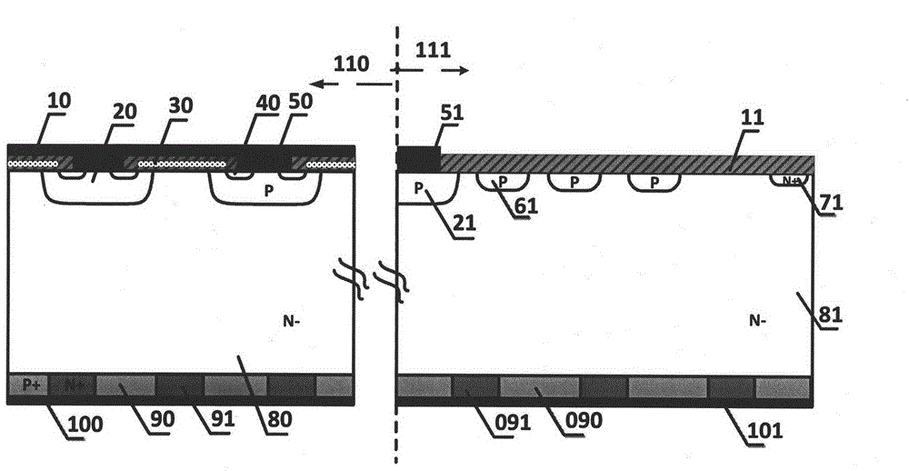
[0022] see image 3 , which shows a collector-short-circuit planar IGBT structure with integrated diodes, including a cell region (110) and a terminal region (111) surrounding the cell region (110), belonging to the technical field of power semiconductor devices. The cell region (110) includes an insulating layer (10), a polysilicon gate (30), an emitter metal (50), a P-body region (20), an emitter N + District (40), N - Drift region (80), collector P + region (90) and collector region (100); terminal region (111) includes main junction (21), field limiting ring (61), channel stop ring (71), N - Drift zone (81), N + Collector short-circuit region (91), emitter metal (51), collector metal (101) and insulating layer (11).

[0023] image 3 The structure shown is the same as figure 1 The structure shown differs in the size of the main junction area. image 3 The main junction area of ​​the structure is large enough to make the current capacity of the integrated diode large...

Embodiment 2

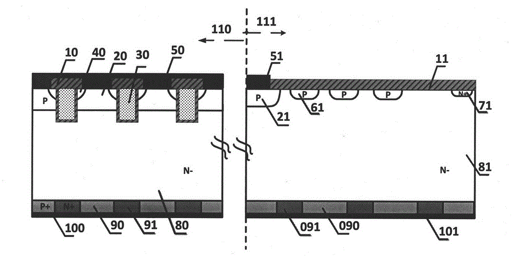
[0028] see Figure 4 , showing a collector-short-circuited trench-gate IGBT structure with integrated diodes, including a cell region (110) and a terminal region (111) surrounding the cell region (110), belonging to the technical field of power semiconductor devices . The cell region (110) includes an insulating layer (10), a polysilicon gate (30), an emitter metal (50), a P-body region (20), an emitter N + District (40), N - Drift region (80), collector P + region (90) and collector region (100); terminal region (111) includes main junction (21), field limiting ring (61), channel stop ring (71), N - Drift zone (81), N + An anode short circuit area (91), an emitter metal (51), a collector metal (101) and an insulating layer (11).

[0029] Figure 4 The structure shown is the same as figure 2 The structure shown differs in the size of the main junction area. Figure 4 The main junction area of ​​the structure is large enough to make the current capacity of the integrat...

Embodiment 3

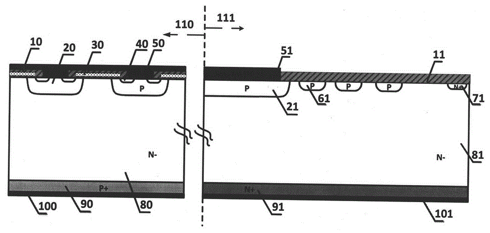
[0034] see Figure 5 , which shows a collector-short-circuited planar IGBT structure integrating JBS / MPS diodes, including a cell region (110) and a terminal region (111) surrounding the cell region (110), belonging to power semiconductor device technology field. The cell region (110) includes an insulating layer (10), a polysilicon gate (30), an emitter metal (50), a P-body region (20), an emitter N + District (40), N - Drift region (80), collector P + region (90) and collector region (100) termination region (111) including main junction (21), field limiting ring (61), channel stop ring (71), N - Drift zone (81), N + An anode short circuit area (91), an emitter metal (51), a collector metal (101) and an insulating layer (11).

[0035] Figure 5 The structure shown is the same as image 3 The difference in the shown structures is that the main junction structure is different, and the type of integrated diode formed is different. image 3 The structure adopts P-type ma...


PUM


Abstract

The invention discloses a collector-electrode short-circuit IGBT structure integrating a diode. The structure includes a cellular area (110) and a terminal area (111) surrounding the cellular area (110) and belongs to the technical field of power semiconductor devices, wherein the cellular area (110) includes an insulating layer (10), polycrystalline silicon gates (30), emitting-electrode metal (50), P-body areas (20), an emitting-electrode N+ area (40), an N- drift area (80), an collector-electrode P+ area (90) and a collector-electrode area (100). The terminal area (111) includes a main junction (21), field limiting rings (61), a channel cutoff ring (71), an N- drift area (81), an N+ collector-electrode short-circuit area (91), emitting-electrode metal (51), collector-electrode metal (101) and an insulating layer (11). The main junction (21), the N- drift area (81) and a collector-electrode N+ area (91) form an antiparallel PiN diode. The structure not only reduces the overall area and packaging cost of a device, but also improves the switching speed of the device and overcoming a reverse-blocking effect of traditional collector-electrode short circuits.

Description

technical field [0001] The invention relates to semiconductor power device technology. Background technique [0002] Insulated-Gate Bipolar Transistor IGBT (Insulated-Gate Bipolar Transistor) is a new type of high-power device, which combines the low on-resistance characteristics of bipolar transistors and the gate voltage control characteristics of MOSFETs, and improves the device by using the conductance modulation effect. The situation that withstand voltage and on-resistance are mutually restrained has the advantages of high voltage, high current, high frequency, high power integration density, large input impedance, small on-resistance, and low switching loss. Such characteristics and advantages make IGBT widely used in many fields such as frequency conversion home appliances, new energy and smart grid. [0003] For the traditional IGBT structure, due to the conductance modulation effect formed by the hole injection of the collector, the turn-off speed of the device is...

Claims


Application Information

Patent Timeline
Patent Type & Authority Applications(China)
IPC IPC(8): H01L29/739H01L29/06
CPCH01L29/66333H01L29/0821
Inventor 何志谢刚
Owner FOSHAN XINGUANG SEMICON
Why Eureka
Try Eureka