Super-junction device

A super-junction device and device technology, applied in the field of semiconductor integrated circuits, can solve the problems of increasing device cost, increasing device specific on-resistance, and high cost, and achieve the effects of reducing epitaxial cost, increasing breakdown voltage, and reducing cost

Inactive Publication Date: 2018-06-05
SHENZHEN SANRISE TECH CO LTD
View PDF3 Cites 5 Cited by
  • Summary
  • Abstract
  • Description
  • Claims
  • Application Information

AI Technical Summary

Problems solved by technology

Therefore, in the prior art, the softness factor can be improved by increasing the thickness of the buffer layer. However, since the buffer layer is formed by an epitaxial process, the thicker the buffer layer, the longer the time

Method used


Image

  • Super-junction device
  • Super-junction device
  • Super-junction device

Examples


no. 1 example

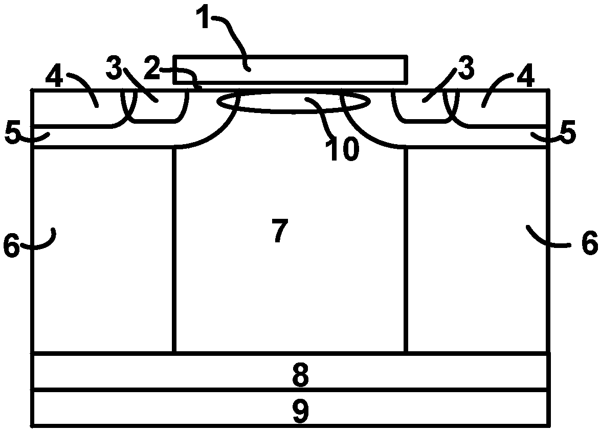
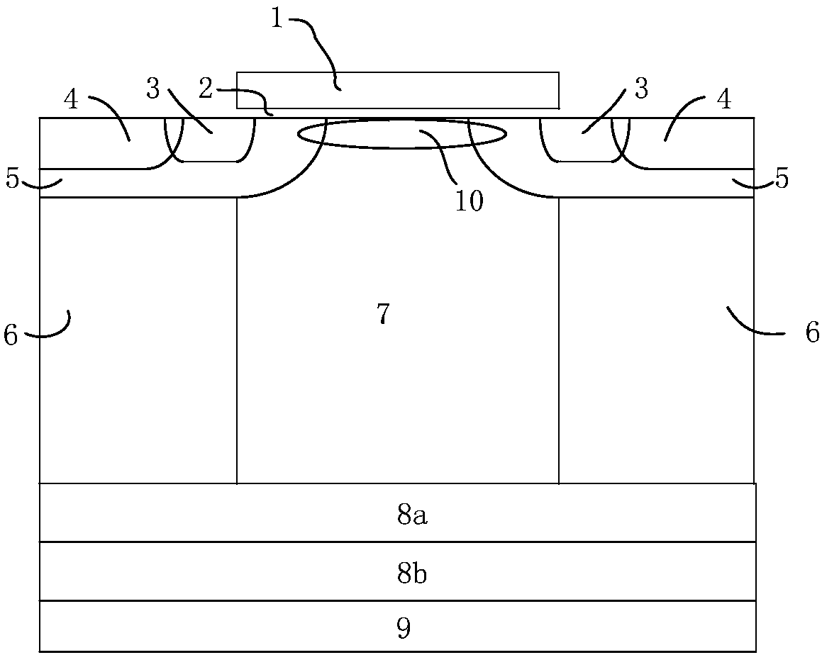
[0074] The three structures are compared below, and the thickness of the drift region of the three structures, that is, the N-type column 7 plus the buffer layer, is 60 μm. The depth of the groove, that is, the P-type pillar 6 is 40 μm. The width of the opening at the top of the trench and the distance between the trenches are the same, and the angle of trench etching and the doping dose of the filled P-type columns are the same.

[0075] The first structure: the width of the drift region, that is, the longitudinal thickness is 40 μm, the width of the buffer layer, that is, the longitudinal thickness is 20 μm, and the doping concentration of the drift region and the buffer layer are the same, that is, 2.93e15 / cm 3 .

[0076] The second structure: the width of the drift region is 40μm, the buffer layer is divided into two layers, the first layer is image 3 The width of the second buffer sublayer 8a shown is 10 μm, and the corresponding doping concentration is 1.0e15 / cm 3 , th...


PUM


Abstract

The invention discloses a super-junction device. The super-junction device comprises a super-junction structure, channel regions, a buffer layer, source regions and a drift region; first conductive type columns and second conductive type columns are alternately arranged so as to form the super-junction structure; a drain region is formed by a semiconductor substrate at the bottom of the buffer layer; the source regions are formed at the surfaces of the channel regions; the drift region, the channel regions and the second conductive type columns form a parasitic body diode; the first buffer sub-layer and a second sub-layer are stacked together to form the buffer layer; the doping concentration of the second sub-layer is lower than the doping concentration of the first conductivity type columns; the softness factor of the reverse recovery of the super-junction device can be increased by adjusting the doping concentration of the second buffer sub-layer; the doping concentration of the first buffer sub-layer is higher than the doping concentration of the second buffer sub-layer; and the specific on-resistance of the super-junction device can be maintained or decreased by adjusting thedoping concentration of the first buffer sub-layer. With the super-junction device of the invention adopted, the softness factor of the reverse recovery can be improved, the cost of the device and thespecific on-resistance of the device can be reduced, and the breakdown voltage of the device can be improved.

Description

technical field [0001] The invention relates to a semiconductor integrated circuit, in particular to a super junction device. Background technique [0002] The super junction structure is composed of alternately arranged N-type pillars and P-type pillars. If the superjunction structure is used to replace the N-type drift region in the vertical double-diffused MOS transistor (Vertical Double-diffused Metal-Oxide-Semiconductor, VDMOS) device, the conduction path is provided through the N-type column in the conduction state, and when the conduction The P-type column does not provide a conduction path; in the off state, the PN column jointly bears the reverse bias voltage, forming a super-junction metal-oxide-semiconductor field-effect transistor (Metal-Oxide-Semiconductor Field-Effect Transistor, MOSFET). Such as figure 1 Shown is a structural diagram of an existing super-junction device. The super-junction device is a super-junction power device. Here, an N-type super-juncti...

Claims


Application Information

Patent Timeline
IPC IPC(8): H01L29/78H01L29/06H01L29/36
CPCH01L29/7828H01L29/0634H01L29/36
Inventor 曾大杰
Owner SHENZHEN SANRISE TECH CO LTD
Why Eureka
Try Eureka