Method for building analytical model of semiconductor device based on empirical formulas

An empirical formula, semiconductor technology, used in instrumentation, computing, electrical digital data processing, etc.

Active Publication Date: 2018-06-12
NAT UNIV OF SINGAPORE +1
View PDF6 Cites 4 Cited by
  • Summary
  • Abstract
  • Description
  • Claims
  • Application Information

AI Technical Summary

Problems solved by technology

However, the high power characteristics also introduce serious memory effects such as charge trap e...

Method used


Image

  • Method for building analytical model of semiconductor device based on empirical formulas
  • Method for building analytical model of semiconductor device based on empirical formulas
  • Method for building analytical model of semiconductor device based on empirical formulas

Examples


Embodiment Construction

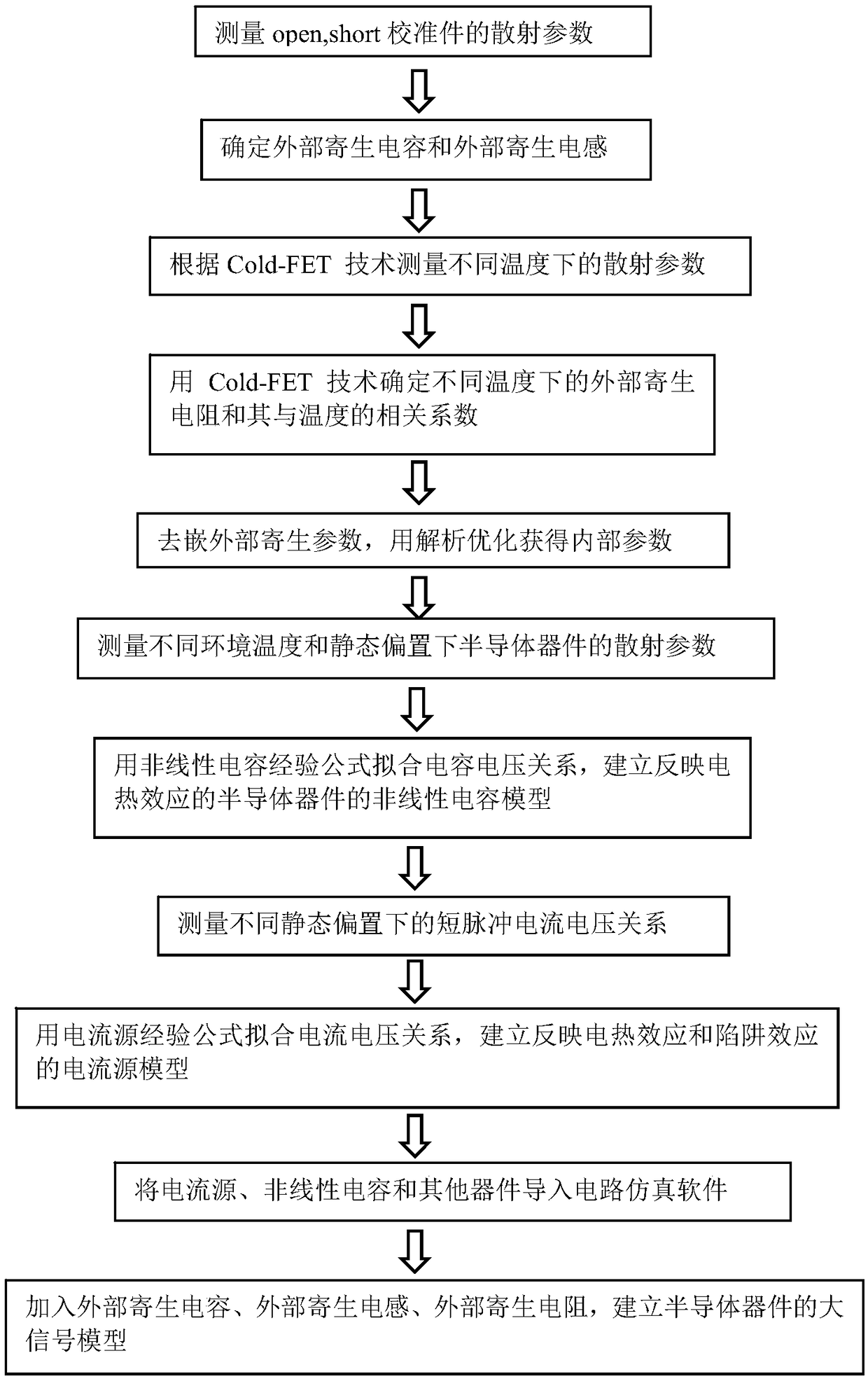
[0028] The specific embodiments of the present invention will be described in detail below in conjunction with the accompanying drawings. In the following description, numerous specific details are set forth in order to provide a thorough understanding of the present invention. However, the present invention can be implemented in many other ways different from those described here, and those skilled in the art can make similar improvements without departing from the connotation of the present invention, so the present invention is not limited by the specific implementations disclosed below.

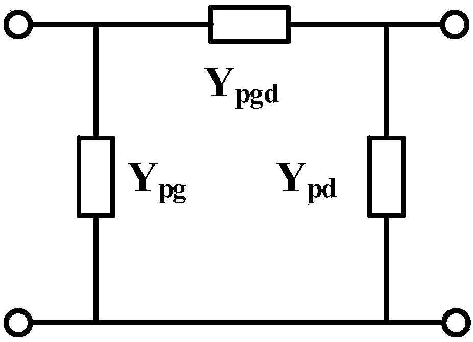
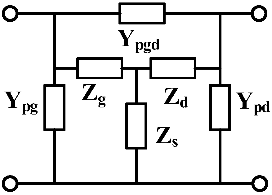
[0029] In some embodiments, the method for establishing an analytical model includes determining internal parameters of a small-signal equivalent model of a high-power transistor and a method for establishing a large-signal model, the method comprising the following steps:

[0030] Measuring the value of a set of scattering parameters (S parameters) of the transistor at multiple ambient t...


PUM


Abstract

The embodiment of the invention includes a method for building an analytical model of a semiconductor device based on the empirical formula of nonlinear capacitance and the empirical formula of a current source. The method includes the following steps of measuring a group of scattering parameters of the semiconductor device under combinations of different environment temperatures and different static biases; determining a group of external parasitic parameters; building a small-signal equivalent circuit model of the semiconductor device; based on the determined external parasitic parameters, removing the external parasitic parameters in the scattering parameters to obtain a group of intrinsic parameters of the small-signal equivalent circuit model of the semiconductor device; using the empirical formula of the nonlinear capacitance to build a nonlinear capacitance model; using the empirical formula of the current source to build a current source model; using the intrinsic parameters, the nonlinear capacitance model and the current source model to build a large-signal equivalent model of the semiconductor device.

Description

technical field [0001] The invention relates to a method for establishing an analytical model of a semiconductor device based on a nonlinear capacitance empirical formula and a current source empirical formula. Background technique [0002] With the development of wide bandgap semiconductor technology and the continuous decline in cost, GaN-based high electron mobility field effect transistors play an increasingly important role in modern radio frequency circuits. Its high power and high frequency characteristics can not only significantly improve the performance of microwave circuits and systems, but also realize high integration and miniaturization of modules. However, the high power characteristic also introduces serious memory effects such as charge trap effect, electrocaloric effect, etc., and these effects have a non-negligible impact on the channel current. Contents of the invention [0003] Due to the high power characteristics, serious memory effects such as char...

Claims


Application Information

Patent Timeline
IPC IPC(8): G06F17/50
CPCG06F30/367G06F30/39
Inventor 郭永新黄安东仲正
Owner NAT UNIV OF SINGAPORE
Why Eureka
Try Eureka