Primary epitaxial growth dual-wavelength semiconductor laser device

An epitaxial growth, dual-wavelength technology, used in semiconductor lasers, semiconductor laser excitation devices, lasers, etc., can solve the problems of low yield of semiconductor bonding processes, many influencing factors, pollution, etc.

Inactive Publication Date: 2018-06-12
CHANGCHUN UNIV OF SCI & TECH
View PDF3 Cites 8 Cited by
  • Summary
  • Abstract
  • Description
  • Claims
  • Application Information

AI Technical Summary

Problems solved by technology

Other methods to achieve dual-wavelength lasing often require a secondary epitaxy process, or need to be combined with the bonding process for processing. The yield rate of the semiconductor bonding process is relatively low, and there are

Method used


Image

  • Primary epitaxial growth dual-wavelength semiconductor laser device
  • Primary epitaxial growth dual-wavelength semiconductor laser device
  • Primary epitaxial growth dual-wavelength semiconductor laser device

Examples


Embodiment 1

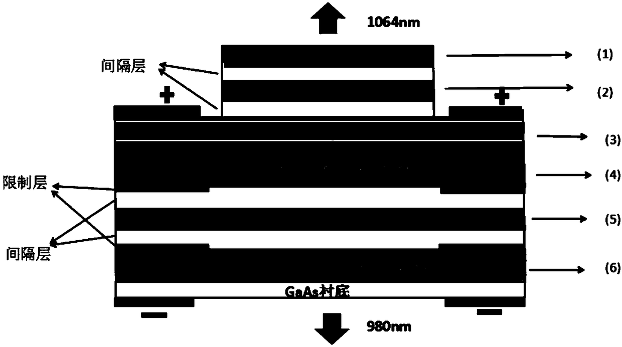
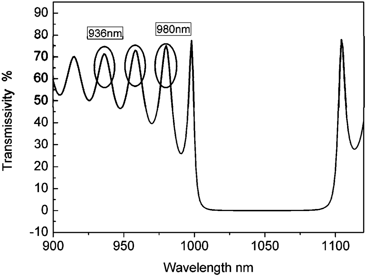
[0046] In this embodiment, the pump light vertical cavity and the excited vertical cavity respectively adopt an integrated vertical cavity structure combining a 980nm vertical cavity and a 1064nm vertical cavity, and the 980nm vertical cavity includes two parts of GaAs / Al 0.9 GaAs DBR, AlGaAs spacer layer, InGaAs / GaAs multi-quantum active region, oxidation confinement layer. 1064nm vertical cavity includes upper and lower parts GaAs / Al 0.9 GaAs DBR, AlGaAs spacer layer, InGaAs / GaAs multi-quantum active region, in order to make the 980nm vertical cavity emit light simultaneously, so the design of the lower DBR is 22 pairs, and the reflectivity is 99.86%. Considering the lower DBR of the 1064nm vertical cavity The reflection of 980nm light is affected, so when using Crosslight software to simulate, the lower DBR of the 1064nm vertical cavity is added to the simulated structure, such as Figure 11 As shown, optimize the number of DBRs on the 980nm vertical cavity, and determine ...

Embodiment 2

[0048] In this embodiment, the pump light vertical cavity and the excited vertical cavity respectively adopt an integrated vertical cavity structure combining a 936nm vertical cavity and a 1064nm vertical cavity, and the 936nm vertical cavity includes two parts of GaAs / Al 0.9 GaAs DBR, AlGaAs spacer layer, InGaAs / GaAs multi-quantum active region, oxidation confinement layer. 1064nm vertical cavity includes upper and lower parts GaAs / Al 0.9 GaAs DBR, spacer layer, InGaAs / GaAs multi-quantum active region, DBR logarithms designed for pump light sources of different wavelengths are different. In order to make the 936nm vertical cavity emit light simultaneously in the upper and lower directions, the number of lower DBRs is designed to be 21 pairs. The ratio is 99.835%, and considering the influence of the lower DBR of the 1064nm vertical cavity on the reflection of 936nm light, the lower DBR of the 1064nm vertical cavity is also added to the simulated structure during the simulatio...


PUM

PropertyMeasurementUnit
Wavelengthaaaaaaaaaa

Abstract

The invention discloses a primary epitaxial growth dual-wavelength semiconductor laser device which comprises a pump light vertical cavity, an excited vertical cavity and a GaAs substrate. Laser lightwith adjustable output optical power can be simultaneously generated by the pump light vertical cavity in the up-down directions, emergent laser light in the upper direction is used as pump light tobe transmitted into the excited vertical cavity, lasing of laser devices of the excited vertical cavity can be pumped by the light, accordingly, dual-wavelength lasing of integrated vertical cavitiescan be implemented, dual-wavelength laser light can be subjected to emergence from the integrated vertical cavities in the upper direction and the lower direction, and the pump light vertical cavity and the excited vertical cavity are formed by means of primary epitaxial growth.

Description

technical field [0001] The invention belongs to the field of semiconductor lasers, in particular to a single epitaxial growth double-wavelength semiconductor laser. Background technique [0002] As one of the core devices in the field of optoelectronics, semiconductor lasers have the advantages of small size and easy integration. It is widely used in the field of laser communication and pump source. With the improvement of the preparation process, the isotropic performance of semiconductor lasers has been greatly improved, and the semiconductor lasers with high integration effect that can realize lasing at two wavelengths are particularly attractive. This easy-to-integrate semiconductor laser can realize dual-wavelength lasing. The lasing wavelength can be freely selected, and the lasing power of the two wavelengths can be adjusted as required. Among them, 980nm and 1064nm lasers can be used in the medical field at the same time, using different wavelength characteristics ...

Claims


Application Information

Patent Timeline
IPC IPC(8): H01S5/183H01S5/04H01S5/187H01S5/34
CPCH01S5/18397H01S5/041H01S5/187H01S5/34
Inventor 王海珠侯春鸽范杰邹永刚马晓辉李洋赵鑫张贺王小龙
Owner CHANGCHUN UNIV OF SCI & TECH
Why Eureka
Try Eureka