High-speed high-voltage level conversion circuit applied to GaN gate drive

A conversion circuit and gate drive technology, applied in the direction of logic circuit interface device, logic circuit connection/interface layout, etc., can solve the problems of ground current consumption, consumption of ground current, high current power consumption, etc. Current consumption, size reduction, cost saving effect

Active Publication Date: 2018-06-12
拓尔微电子股份有限公司
View PDF9 Cites 15 Cited by
  • Summary
  • Abstract
  • Description
  • Claims
  • Application Information

AI Technical Summary

Problems solved by technology

However, there will be unnecessary current consumption to ground after the level shift is complete, for example when V IN When the high level is maintained, the left-to-ground branch will continue to conduct, and will continue to consume I d The ground current, resulting in a large current consumption

Method used


Image

  • High-speed high-voltage level conversion circuit applied to GaN gate drive
  • High-speed high-voltage level conversion circuit applied to GaN gate drive
  • High-speed high-voltage level conversion circuit applied to GaN gate drive

Examples


Embodiment 1

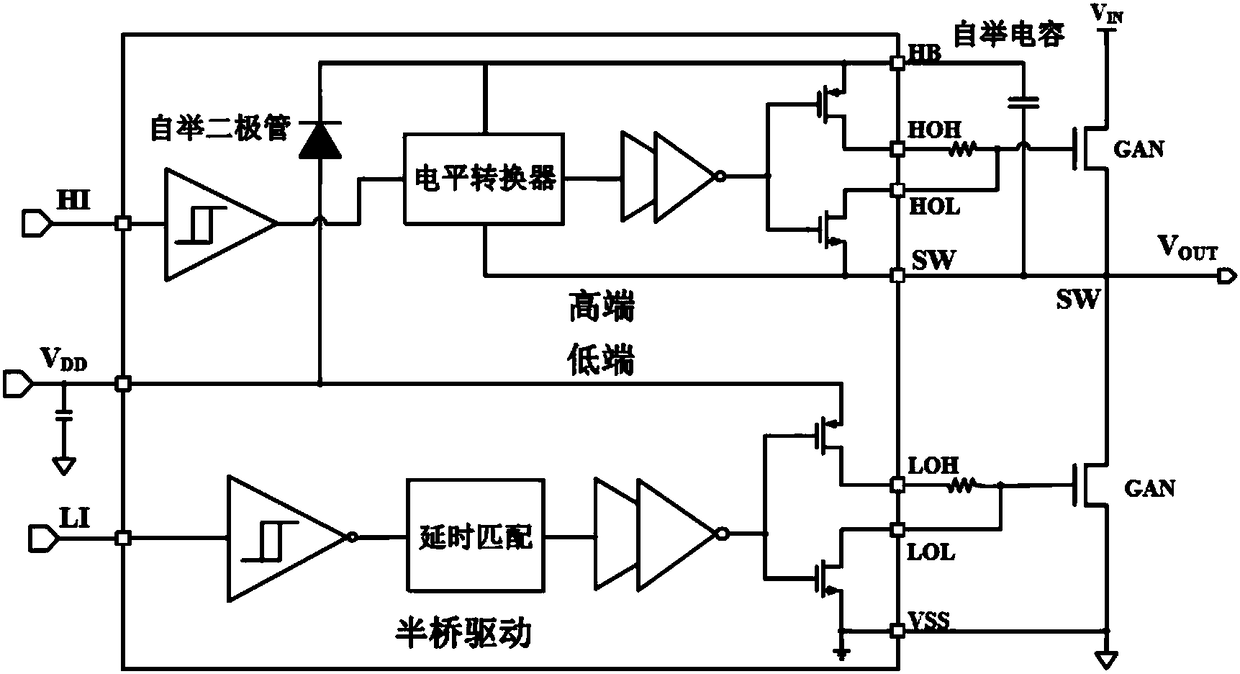
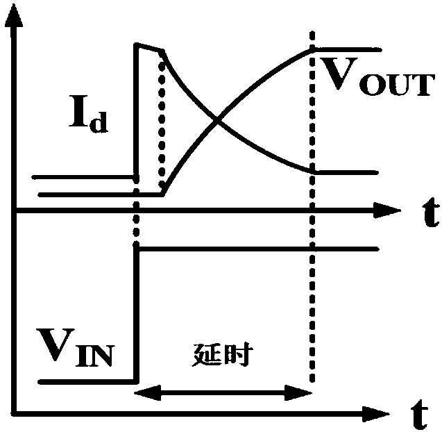
[0051] Image 6 A high-speed high-voltage level conversion circuit applied to GaN driving according to the first embodiment of the present invention is shown.

[0052] Such as Image 6 As shown, the present invention provides a high-speed high-voltage level conversion circuit applied to GaN gate drive, including: an input circuit 601, a first PMOS transistor 602 (that is, Image 6 MP1 in), the level conversion circuit 603 and the shaping circuit 604; the first end of the input circuit 601 is connected to the first end of the level conversion circuit 603 at the first node NH, and the second end is connected to the first PMOS at the second node A The drain of the transistor 602, the gate of the first PMOS transistor 602 is connected to the first power supply line, the source of the first PMOS transistor 602 is connected to the second terminal of the level conversion circuit 603 at the third node NL, and the level conversion circuit 603 Connected to the second power line, the s...

Embodiment 2

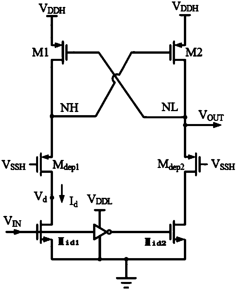
[0082] Figure 8 A high-speed high-voltage level conversion circuit applied to GaN driving according to the second embodiment of the present invention is shown.

[0083] Such as Figure 8 As shown, the present invention provides a high-speed high-voltage level conversion circuit 803 applied to GaN gate drive, including: an input circuit 801, a first PMOS transistor 802 (that is, Figure 8 MP1 in), the level conversion circuit 803 and the shaping circuit 804; the first end of the input circuit 801 is connected to the first end of the level conversion circuit 803 at the first node NH, and the second end is connected to the first PMOS at the first node A The drain of the transistor 802, the gate of the first PMOS transistor 802 is connected to the first power supply line, the source of the first PMOS transistor 802 is connected to the second terminal of the level conversion circuit 803 at the third node NL, and the level conversion circuit 803 Connected to the second power line...


PUM


Abstract

The invention discloses a high-speed high-voltage level conversion circuit applied to a GaN gate drive. The high-speed high-voltage level conversion circuit comprises an input circuit, a first PMOS (P-channel Metal Oxide Semiconductor) transistor, a level conversion circuit and a shaping circuit, wherein a first end of the input circuit is connected to a first end of the level conversion circuit at a first node; a second end of the input circuit is connected to a drain electrode of the first PMOS transistor at a second node; a gate electrode of the first PMOS transistor is connected to a firstpower line; a source electrode of the first PMOS transistor is connected to a second end of the level conversion circuit at a third node; the level conversion circuit is connected to a second power line; a second end of the level conversion circuit is connected to an input end of the shaping circuit at the third node; the shaping circuit is connected to the first power line and the second power line; an output end of the shaping circuit is connected to a first end of a power device at a fourth node; and the power device is connected to the first power line and the third power line.

Description

technical field [0001] The invention belongs to the field of integrated circuit design, and more specifically relates to a high-speed high-voltage level conversion circuit applied to GaN gate driving. Background technique [0002] Traditional power electronic power devices based on silicon materials have gradually approached their theoretical limits, and it is difficult to meet the development needs of high frequency and high power density of power electronic technology. Compared with traditional Si devices, GaN devices show their advantages in on-resistance and gate charge, which can enable power converters to achieve smaller volume, higher frequency and higher efficiency, so that they can be used in automotive, communication, industrial It has broad application prospects in other fields. The increase of switching frequency can not only effectively reduce the size of capacitors, inductors and transformers in the system circuit, but also suppress interference, reduce ripple...

Claims


Application Information

Patent Timeline
Patent Type & Authority Applications(China)
IPC IPC(8): H03K19/0175
CPCH03K19/017509
Inventor 郭建平张弘
Owner 拓尔微电子股份有限公司
Why Eureka
Try Eureka