Fabrication method of display panel, display panel and display device

一种显示面板、基板的技术,应用在最终产品制造、可持续制造/加工、半导体/固态器件制造等方向,能够解决OLED面板出光效率影响、降低OLED显示出光效率、OLED显示画质差等问题,达到提高出光效率及柔性显示效果、改善干涉效应的效果

Active Publication Date: 2018-06-22
WUHAN CHINA STAR OPTOELECTRONICS SEMICON DISPLAY TECH CO LTD
View PDF10 Cites 11 Cited by
  • Summary
  • Abstract
  • Description
  • Claims
  • Application Information

AI Technical Summary

Problems solved by technology

[0003] The current mainstream thin-film packaging technology uses a mix of inorganic and organic films to achieve water and oxygen barriers for OLED devices. However, the introduction of thin-film packaging has an impact on the light output efficiency of OLED panels. The refractive index of the thin film layer and the inorganic layer are different, and a microcavity will be formed between the cathode and the anode of the OLED. The light emitted by the OLED will interfere in these microcavities, thereby reducing the light efficiency of the OLED and the CIE of the display light. Offset, etc., resulting in poor display quality of OLED

Method used


Image

  • Fabrication method of display panel, display panel and display device
  • Fabrication method of display panel, display panel and display device
  • Fabrication method of display panel, display panel and display device

Examples


Embodiment Construction

[0044] The following will clearly and completely describe the technical solutions in the embodiments of the present invention with reference to the accompanying drawings in the embodiments of the present invention. Obviously, the described embodiments are only some, not all, embodiments of the present invention. Based on the embodiments of the present invention, all other embodiments obtained by persons of ordinary skill in the art without creative efforts fall within the protection scope of the present invention.

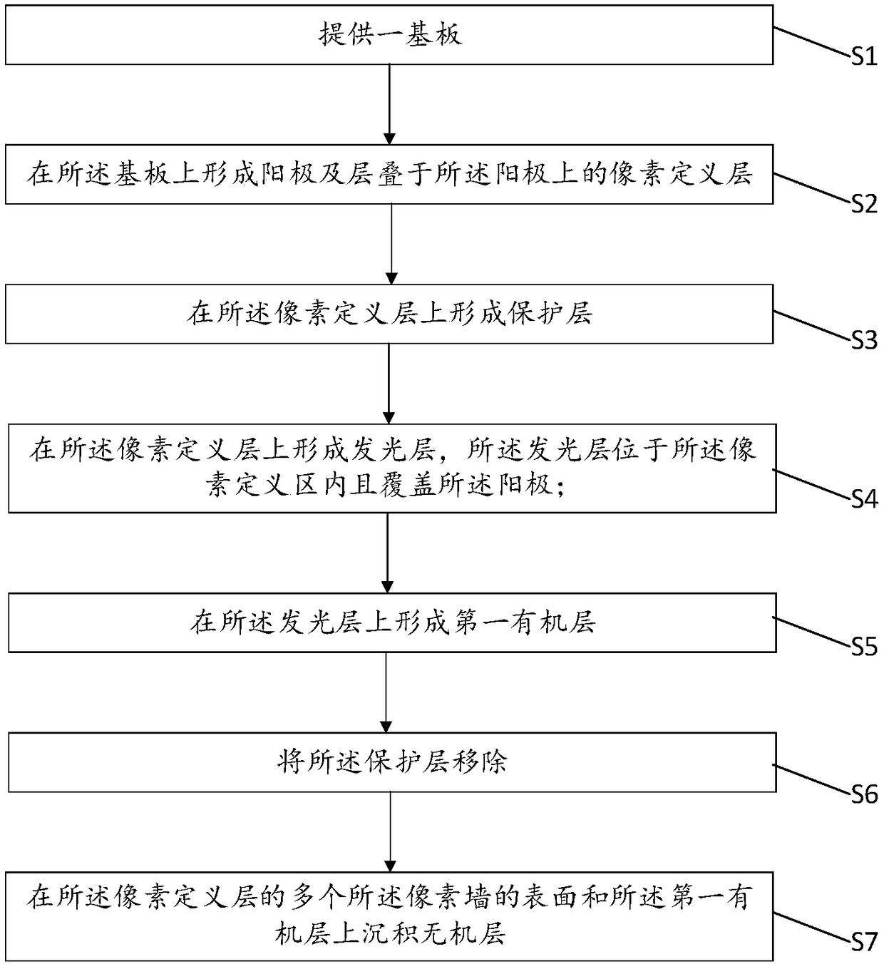
[0045] see figure 1 , a preferred embodiment of the present invention provides a method for preparing a display panel, which is used to prepare an OLED panel, improve the thin film packaging structure of the OLED panel, and improve the display quality. The method includes:

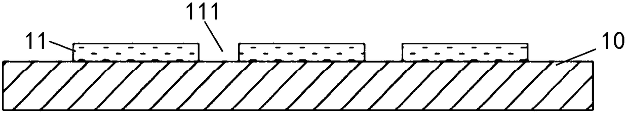
[0046] Please combine figure 2 , step S1 , providing a substrate 10 . In this embodiment, the substrate 10 is made of flexible materials.

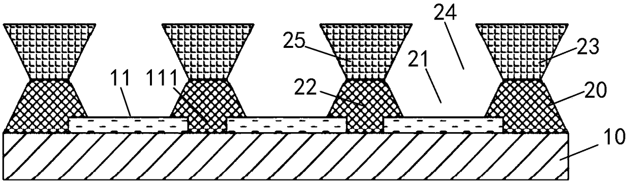
[0047] see also image 3 , step S2 , forming an ...


PUM


Abstract

The invention provides a display panel. The display panel comprises a substrate, positive electrodes, pixel defining layers, light-emitting layers, first organic layers and inorganic layers, wherein the positive electrodes are arranged on the substrate, the pixel defining layers are laminated on the positive electrodes, each pixel defining layer comprises a plurality of pixel walls and pixel defining regions, each pixel defining is arranged between each two pixel walls, the pixel defining regions are exposed out of the positive electrodes, the light-emitting layers are arranged on the pixel defining layers, the light-emitting layers are arranged in the pixel defining regions and cover the positive electrodes, the first organic layers are arranged on the light-emitting layers, each first organic layer comprises a plurality of first bulges, the inorganic layers are arranged on surfaces of the plurality of pixel walls of the pixel defining layers and the first organic layers, each inorganic layer comprises a plurality of second bulges, each second bulge is arranged on one surface, far away from the first organic layer, of the inorganic layer, and each second bulge is corresponding toeach first bulge. The invention also provides a fabrication method of the display panel and a display device.

Description

technical field [0001] The invention relates to the field of display technology, in particular to a method for preparing a display panel, a display panel and a display device. Background technique [0002] Compared with liquid crystal display (LCD, Liquid Crystal Display), Active Matrix Organic Light Emitting Diode (AMOLED, Active Matrix / Organic Light Emitting Diode) display panel has the advantages of high contrast, viewing angle, moving image response speed, etc., which has attracted people's widespread attention. Follow and develop. With the expansion of OLED application fields, new application fields require more flexible OLED displays. At the same time, OLED flexible displays will also have more and more requirements such as: OLED display life, bending radius, bending times, etc. ; OLED flexible display will require thin-film packaging for OLED devices. [0003] The current mainstream thin-film packaging technology uses a mix of inorganic and organic films to achieve ...

Claims


Application Information

Patent Timeline
Patent Type & Authority Applications(China)
IPC IPC(8): H01L27/32H01L51/52H01L51/56
CPCH10K59/121H10K59/122H10K50/84H10K50/85H10K71/00Y02E10/549Y02P70/50H10K50/81H10K50/82H10K50/844H10K77/111
Inventor 夏存军彭斯敏
Owner WUHAN CHINA STAR OPTOELECTRONICS SEMICON DISPLAY TECH CO LTD
Why Eureka
Try Eureka