Vertical double-diffused field-effect transistor and fabrication method thereof

A field-effect transistor and vertical double-diffusion technology, which is applied in semiconductor/solid-state device manufacturing, semiconductor devices, electrical components, etc., can solve problems affecting device performance, improve device performance, reduce parasitic capacitance, and reduce manufacturing costs Effect

Inactive Publication Date: 2018-06-22
深圳市金誉半导体股份有限公司
View PDF3 Cites 0 Cited by
  • Summary
  • Abstract
  • Description
  • Claims
  • Application Information

AI Technical Summary

Problems solved by technology

However, N-type implantation is a full-chip implantation, and non-JFET regions will also be implanted, which will affect device performance.

Method used


Image

  • Vertical double-diffused field-effect transistor and fabrication method thereof
  • Vertical double-diffused field-effect transistor and fabrication method thereof
  • Vertical double-diffused field-effect transistor and fabrication method thereof

Examples


Embodiment Construction

[0027] The following will clearly and completely describe the technical solutions in the embodiments of the present invention. Obviously, the described embodiments are only some of the embodiments of the present invention, rather than all the embodiments. Based on the embodiments of the present invention, all other embodiments obtained by persons of ordinary skill in the art without making creative efforts belong to the protection scope of the present invention.

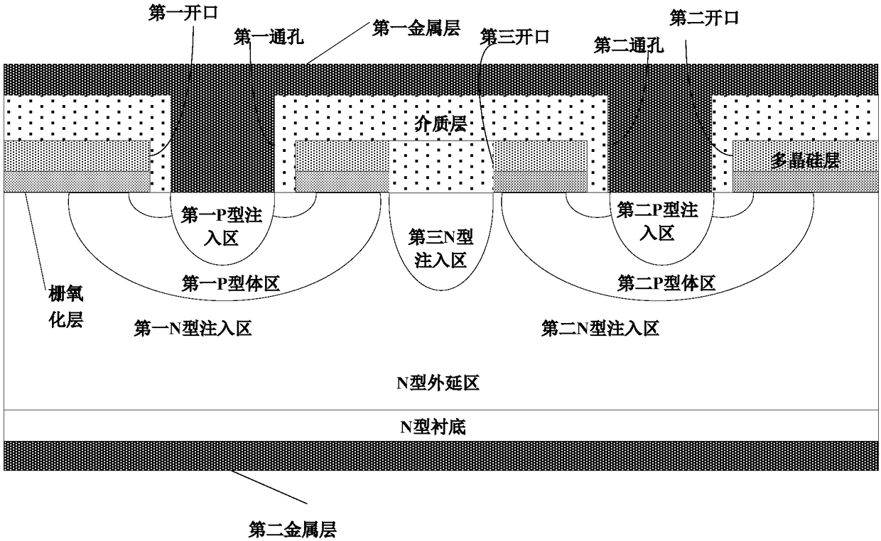
[0028] see figure 1 , figure 1 It is a schematic diagram of the cross-sectional structure of the vertical double-diffused field effect transistor provided by the present invention. The transistor includes an N-type substrate, an N-type epitaxial region formed on the N-type substrate, a first P-type body region and a second P-type body region formed on the surface of the N-type epitaxial region, and is located on the N-type epitaxial region. Two first N-type implanted regions on the surface of the first P-type body ...


PUM


Abstract

A vertical double-diffused field-effect transistor comprises an N-type substrate, an N-type epitaxial region, a first P-type body region, a second P-type body region, two first N-type injection regions, two second N-type injection regions, a third N-type injection region, a first P-type injection region, a second P-type injection region, a grid oxide layer, a poly-silicon layer, a dielectric layer, a first through hole and a second through hole, wherein the first P-type body region and the second P-type body region are formed on a surface of the N-type epitaxial region, the two first N-type injection regions are arranged on a surface of the first P-type body region, the two second N-type injection regions are arranged on a surface of the second P-type body region, the third N-type injection region is arranged on a surface of the N-type epitaxial region, the first P-type injection region is arranged between the two first N-type injection regions, the second P-type injection region is arranged between the two second N-type injection regions, the grid oxide layer and the poly-silicon layer are sequentially formed on the N-type epitaxial region, the first P-type body region, the secondP-type body region, the first N-type injection region and the second N-type injection region, the dielectric layer is formed on the poly-silicon layer and on the first N-type injection region, the second N-type injection region and the third N-type injection region, the first through hole penetrates through the dielectric layer and is corresponding to the first N-type injection region and the first P-type injection region, and the second through hole penetrates through the dielectric layer and is corresponding to the second N-type injection region and the second P-type injection region.

Description

【Technical field】 [0001] The invention relates to the technical field of semiconductor chip fabrication, in particular to a vertical double diffused field effect transistor (VDMOS) and a fabrication method thereof. 【Background technique】 [0002] The drain and source poles of the vertical double diffused field effect transistor (VDMOS) are respectively on both sides of the device, so that the current flows vertically inside the device, increasing the current density, improving the rated current, and the on-resistance per unit area is also small, which is a A very versatile power device. The most important performance parameter of a vertical double diffused field effect transistor (VDMOS) is the operating loss, which can be divided into three parts: conduction loss, cut-off loss and switching loss. The conduction loss is determined by the conduction resistance, the cut-off loss is affected by the reverse leakage current, and the switching loss refers to the loss caused by th...

Claims


Application Information

Patent Timeline
Patent Type & Authority Applications(China)
IPC IPC(8): H01L29/78H01L29/06H01L21/336
CPCH01L29/7802H01L29/0603H01L29/0684H01L29/66712
Inventor 梅小杰李龙杨东邹荣涛杜永琴
Owner 深圳市金誉半导体股份有限公司
Why Eureka
Try Eureka