Negative differential resistance effect device based on gold-ferroelectric monocrystalline system and preparation of device

A technology of negative differential resistance and ferroelectric single crystal, which is applied in the direction of bulk negative resistance effect devices, electrical components, circuits, etc., can solve problems such as failure and achieve excellent spontaneous polarization effect

Active Publication Date: 2018-06-26
TONGJI UNIV
View PDF4 Cites 0 Cited by
  • Summary
  • Abstract
  • Description
  • Claims
  • Application Information

AI Technical Summary

Problems solved by technology

In terms of manufacturing process, the traditional laser etching technology used to ma

Method used


Image

  • Negative differential resistance effect device based on gold-ferroelectric monocrystalline system and preparation of device
  • Negative differential resistance effect device based on gold-ferroelectric monocrystalline system and preparation of device
  • Negative differential resistance effect device based on gold-ferroelectric monocrystalline system and preparation of device

Examples


Embodiment 1

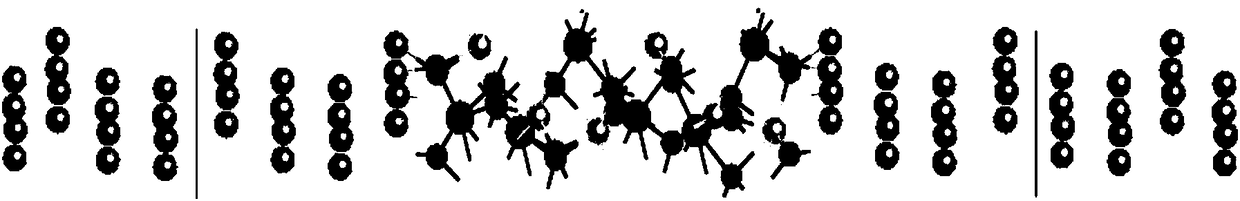
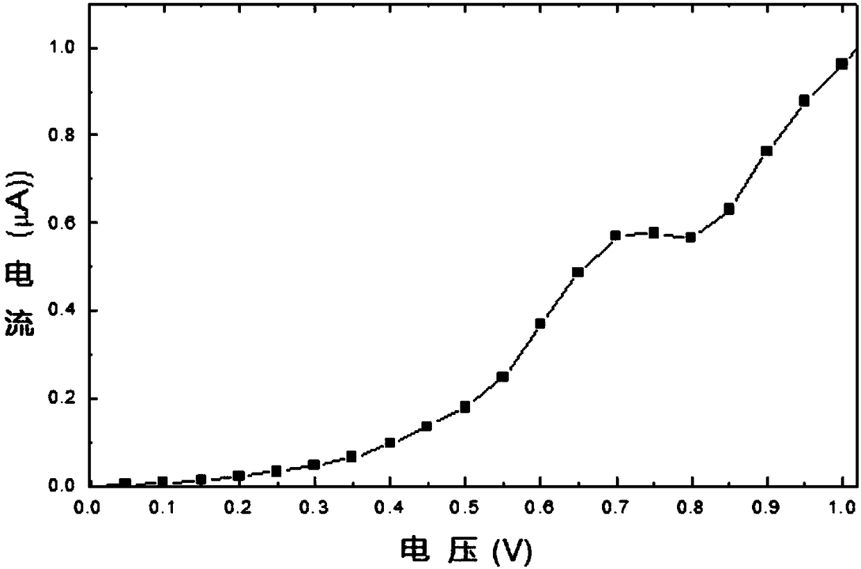
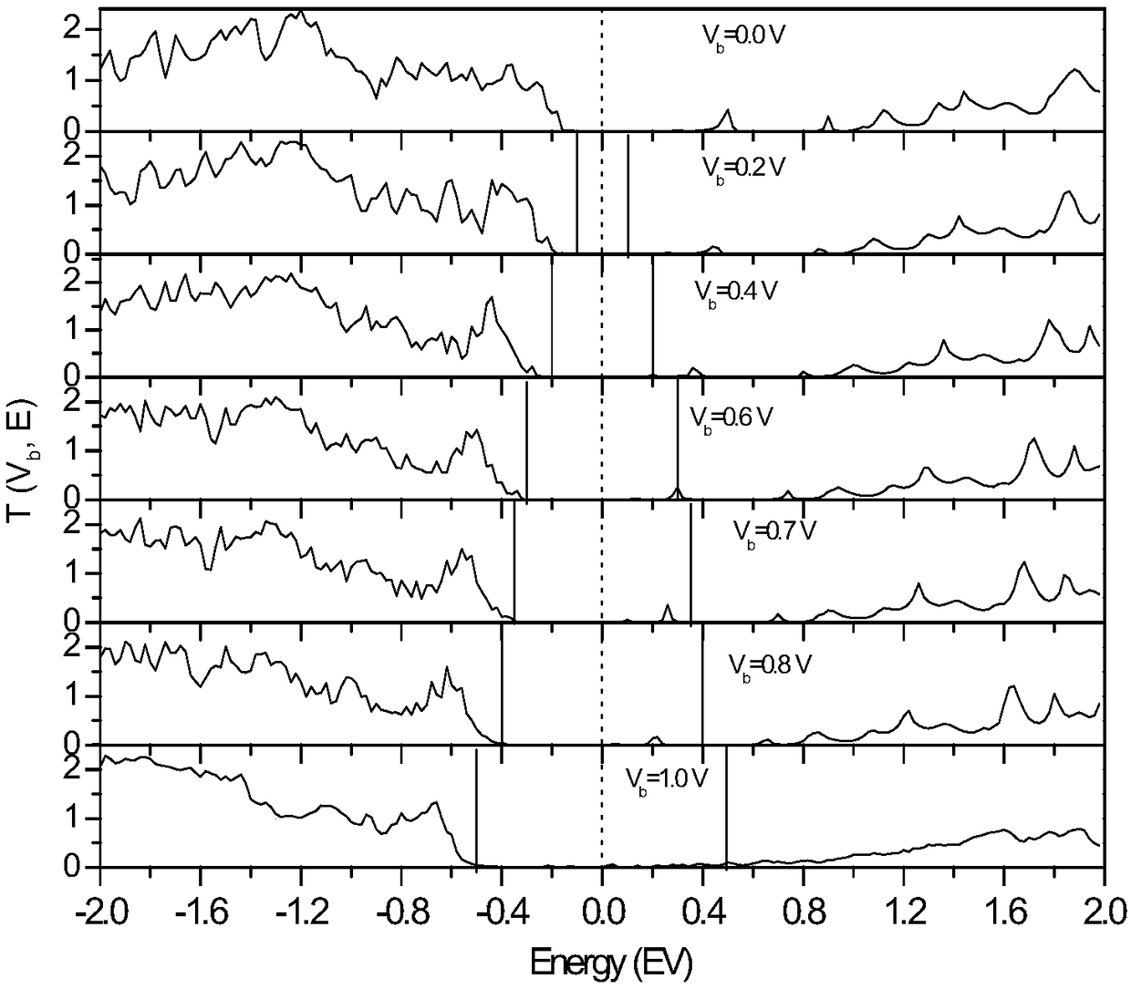
[0022] like figure 1 As shown, a negative differential resistance effect device system based on the gold-ferroelectric single crystal system includes two gold electrodes with a spacing of nanometers as the source and drain, and the ferroelectric single crystal CdPbO 3 as an intermediate scatter zone. Wherein the materials of the left and right electrodes are all gold, and a thin layer of ferroelectric crystals with a thickness of nanometers is arranged sequentially in the z-axis direction and the left and right gold electrodes to form a three-dimensional periodic layered structure, and the ferroelectric single crystal is also in contact with the source. . In the electrical transport of electronic devices, the current is mainly provided by the transmission channel into the transport window. These transmission channels are generated by matching the energy band of the electrode with the energy level of the ferroelectric crystal, where the energy level of the ferroelectric cryst...


PUM


Abstract

The invention relates to a negative differential resistance effect device based on a gold-ferroelectric monocrystalline system and preparation of the device. The negative differential resistance effect device comprises two gold electrodes as source and drain electrodes respectively, ferroelectric monocrystalline arranged between the two gold electrodes by making contact with the electrodes and form an intermediate scattering area, and grids connected to the two sides of the ferroelectric monocrystalline; each of the gold electrodes and the ferroelectric monocrystalline includes a thin layer material positioned in a plane formed by the axis X and the axis Y; and sandwich structures of one gold electrode, ferroelectric monocrystalline and the other gold electrode are arranged regularly alongthe axis Z and form the negative differential resistance effect device. Compared with the prior art, the density of states of 4d tracks of Cd2+ in the CdPbO3 is coupled with the surface state of thegold electrodes (Au), so that a negative differential resistance effect that the current is reduced with increase of the bias within certain bias range is realized, and the device of the invention maybe a candidate of a next generation of high-performance electronic component.

Description

technical field [0001] The invention relates to a negative differential resistance effect device, in particular to a negative differential resistance effect device based on gold-ferroelectric single crystal system and its preparation. Background technique [0002] The semiconductor transistor is one of the greatest inventions in human history. The development and application of traditional silicon-based semiconductor transistors has achieved great success, but the design and manufacture of silicon-based semiconductor transistors is a top-down model. According to Moore's Law, the density of electronic devices is gradually approaching the physical and dimensional limits. Scientists and engineers predict that the actual size of individual silicon-based semiconductor transistors, and the actual distance between them, will be smaller than the wavelength of one electron. Quantum mechanics tells us that the wavelength of an electron is about 10nm. When the size of the transistor i...

Claims


Application Information

Patent Timeline
IPC IPC(8): H01L47/00
CPCH10N80/01H10N80/00
Inventor 张静柯三黄
Owner TONGJI UNIV
Why Eureka
Try Eureka