Eureka AIR delivers breakthrough ideas for toughest innovation challenges, trusted by R&D personnel around the world.

Differential photoelectric detection device and photoelectric test system

A photoelectric detection and differential technology, applied in the field of photoelectric detection, can solve problems such as inability to apply high-frequency laser signals, affect system signal stability, and affect effective signal output, and achieve the effects of reducing implementation costs, simple structure, and increasing bandwidth.

Active Publication Date: 2018-06-29
湖南红太阳新能源科技有限公司
View PDF3 Cites 0 Cited by
  • Summary
  • Abstract
  • Description
  • Claims
  • Application Information

AI Technical Summary

Problems solved by technology

[0004] 1) The output signal of the system is unstable, which will generate a resonance signal and affect the output of the effective signal;
[0005] 2) Due to the large value of the feedback resistor, increasing the amplification factor of the amplifier will also amplify the noise signal, which greatly affects the quality of the system output signal
However, the photoelectric differential detector directly uses a transimpedance amplification circuit, and a resistor is set at the front end of the amplifier, so the transimpedance resistance value must be set to a small value when used, which can only be used in the application of low frequency signals, and for high frequency signals , the combination of the resistor and the photodiode at the front end of the amplifier will oscillate, which will affect the stability of the system signal, that is, it cannot be applied to the application of high-frequency laser signals, and the bandwidth of the entire detector is very narrow

Method used


Image

  • Differential photoelectric detection device and photoelectric test system
  • Differential photoelectric detection device and photoelectric test system
  • Differential photoelectric detection device and photoelectric test system

Examples


Embodiment Construction

[0028] The present invention will be further described below in conjunction with the accompanying drawings and specific preferred embodiments, but the protection scope of the present invention is not limited thereby.

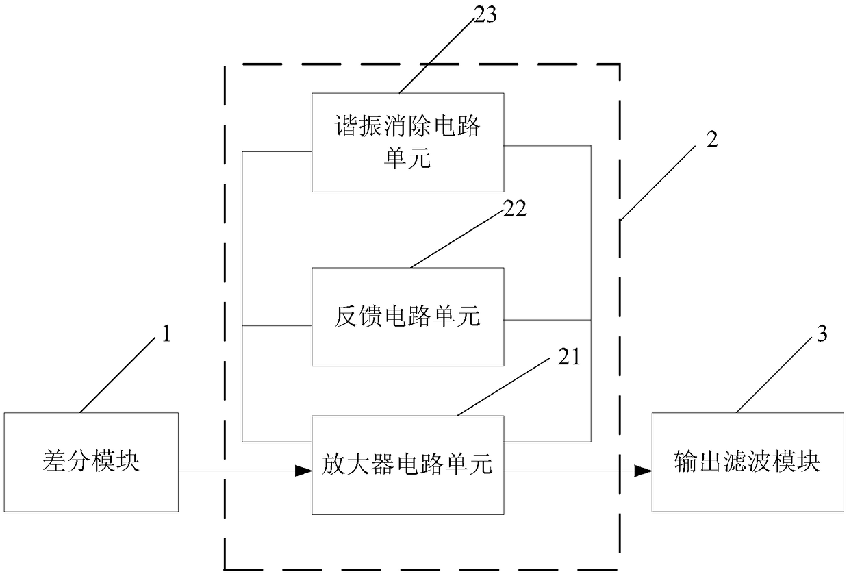
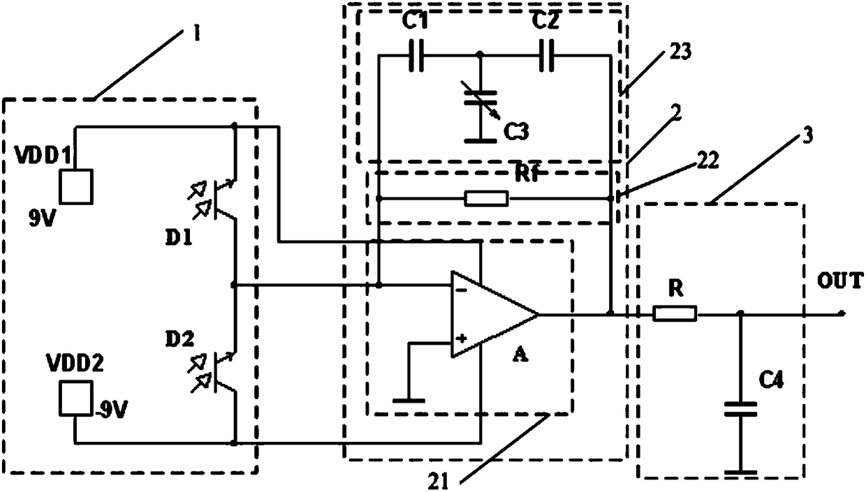
[0029] Such as figure 1 As shown, the differential photoelectric detection device in this embodiment includes a differential module 1 and an amplifying module 2 connected to each other. The differential module 1 is connected to two optical signals for differential calculation and outputs a photocurrent signal. The amplifying module 2 is connected to the output of the differential module 1. The photocurrent signal is converted into a voltage signal and output after amplifying, and also includes an output filter module 3 arranged at the output end of the amplification module 2, and the output filter module 3 filters out the resonance signal and the high-frequency noise signal in the output signal of the amplification module 2, Output the final detection signal.

...


PUM


Abstract

The invention discloses a differential photoelectric detection device and a photoelectric test system. The device comprises a differential module and an amplification module which are connected with each other, wherein the differential module is connected with two paths of optical signals for differential operation, and outputs photocurrent signals; the amplification module is connected with the photocurrent signals output by the differential module, converts the photocurrent signals into voltage signals and amplifies the voltage signals for output. The device further comprises an output filtering module arranged at the output end of the amplification module, wherein the output filtering module filters out high-frequency noise signals in the output signals of the amplification module, or filters out high-frequency noise signals and resonance signals in the output signals of the amplification module, and outputs a final detection signal; and the system comprises an acousto-optic generating device, the differential photoelectric detection device and a demodulation module. The differential photoelectric detection device and the photoelectric test system have the advantages of simple structure, low cost, high bandwidth, low noise, no resonance, high stability and the like.

Description

technical field [0001] The invention relates to the technical field of photoelectric detection, in particular to a differential photoelectric detection device and a photoelectric test system. Background technique [0002] In laser testing and other technologies, it is often necessary to modulate the laser, such as the test of the Farad rotation angle, Bell-Bloom optical magnetic resonance test, etc. During the test, in order to obtain the photocurrent signal required for the test, it is necessary to perform differential processing on the same laser beam for photodetection. At present, photodetectors usually first differentiate the same laser beam, and then convert it into a voltage signal by the amplifier circuit and amplify it. If the feedback resistor value in the amplifier circuit is set to a small value, the bandwidth of the entire photodetector is small. In the test process, the modulation frequency is usually required to be high, such as the optical magnetic resonance...

Claims


Application Information

Patent Timeline
IPC IPC(8): G01J1/44
CPCG01J1/44G01J2001/4242G01J2001/446
Inventor 陈林李瑫刘帅曹华翔袁昭岚
Owner 湖南红太阳新能源科技有限公司
Why Eureka
Eureka Blog
Learn More