Preparation method of chip packaging body and chip packaging body

A chip packaging and chip technology, which is applied in the field of integrated circuit chip packaging, can solve the problems of low efficiency in the interconnection process between flip chips and circuit boards, and achieve the effect of improving efficiency and improving interconnection efficiency

Active Publication Date: 2018-06-29
NANTONG FUJITSU MICROELECTRONICS
View PDF4 Cites 3 Cited by
  • Summary
  • Abstract
  • Description
  • Claims
  • Application Information

AI Technical Summary

Problems solved by technology

[0003] Flip chip, also known as flip chip, is to deposit solder on the I / O pad, and then flip the flip chip to heat and use the molten solder to combine with the circuit board, using its superior electrical and thermal properties to It achieves technical effects such as improving chip packaging efficiency and reducing package size, and is widely used in integrated circuits, but the current interconnection process efficiency of flip chips and circuit boards is low

Method used


Image

  • Preparation method of chip packaging body and chip packaging body
  • Preparation method of chip packaging body and chip packaging body
  • Preparation method of chip packaging body and chip packaging body

Examples


Embodiment Construction

[0023] The following will clearly and completely describe the technical solutions in the embodiments of the present invention with reference to the drawings in the embodiments of the present invention.

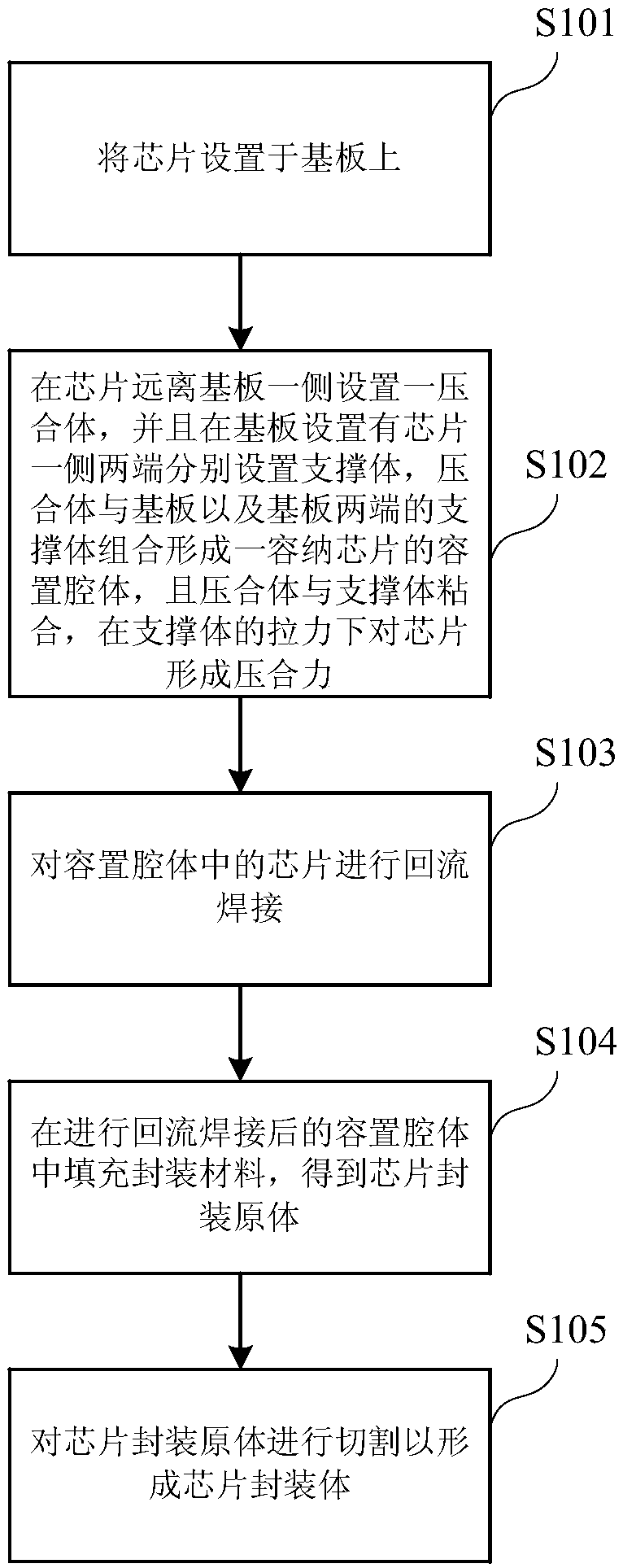
[0024] see figure 1 , figure 1 is a schematic flow chart of the first embodiment of the chip package manufacturing method of the present invention.

[0025] S101: disposing the chip on the substrate;

[0026] In this embodiment, the substrate is the carrier platform of the chip. Since the chip is provided with many precision parts and circuit pins, and the cost of chip preparation is expensive, in order to protect the structural integrity of the chip, the chip is arranged on the substrate. The substrate is connected to the external circuit. While providing sufficient protection strength for the chip, the plasticity of the substrate is higher than that of the chip, so the substrate and the connection structure of the external circuit can be adapted to each other to realize th...


PUM


Abstract

The invention relates to the technical field of integrated circuit chip packaging, and discloses a preparation method of a chip packaging body and the chip packaging body. The method comprises the following steps: arranging a chip on a base plate; arranging a press-fit body on one side, far away from the base plate, of the chip; respectively arranging supporting bodies on two ends of the side, provided with the chip, of the base plate; combining the press-fit body, the base plate and the supporting bodies at the two ends of the base plate to form an accommodating cavity for accommodating the chip; adhering the press-fit body with the supporting bodies; forming press-fit force to the chip under tensions of the supporting bodies; performing reflow soldering on the chip in the accommodating cavity; filling the accommodating cavity subjected to the reflow soldering with a packaging material to obtain a chip packaging original body; cutting the chip packaging original body to form the chippackaging body. According to the method, the efficiency of a chip packaging body preparation process can be improved.

Description

technical field [0001] The invention relates to the technical field of integrated circuit chip packaging, in particular to a method for preparing a chip package and the chip package. Background technique [0002] The inventors of the present invention discovered in the long-term research and invention process that an integrated circuit (Integrated Circuit, IC) is a microelectronic device with a very high assembly density, and a large number of transistors, resistors, capacitors, inductors and other components and wiring are placed in the The interconnection in a limited area forms a whole and becomes a microelectronic device with the required circuit function. It has the advantages of small size, light weight, few lead wires and solder joints, and low cost. It is suitable for large-scale industrial production and is used in civilian electronics. Equipment, such as radios, televisions, computers, etc., are widely used in military, communication, and remote control. [0003] ...

Claims


Application Information

Patent Timeline
Patent Type & Authority Applications(China)
IPC IPC(8): H01L21/50H01L21/56H01L21/603
CPCH01L2224/16225H01L21/50H01L21/561H01L21/563H01L24/81H01L2224/81815
Inventor 汪民
Owner NANTONG FUJITSU MICROELECTRONICS
Why Eureka
Try Eureka