Heterogeneous integration method and heterogeneous integrated device of compound semiconductor and silicon-based complementary metal oxide semiconductor wafer

A technology of oxide semiconductors and complementary metals, which is applied in semiconductor devices, semiconductor/solid-state device manufacturing, electric solid-state devices, etc., can solve the problems that different material devices cannot be mixed and integrated, process compatibility cannot be achieved, and device selection is limited, etc., to achieve Facilitate automatic application, improve production efficiency, and simple process

Active Publication Date: 2022-04-05
INST OF MICROELECTRONICS CHINESE ACAD OF SCI
View PDF5 Cites 0 Cited by
  • Summary
  • Abstract
  • Description
  • Claims
  • Application Information

AI Technical Summary

Problems solved by technology

Since silicon-based semiconductor CMOS chips and compound semiconductor semiconductor chips are difficult to produce in the same fab, process compatibility cannot be achieved. However, if the two are organically combined to break through the limited selection of devices in the field of integrated circuit design, various materials and devices The problem of not being able to mix and integrate will surely achieve a substantial improvement in integrated circuit design and performance

Method used


Image

  • Heterogeneous integration method and heterogeneous integrated device of compound semiconductor and silicon-based complementary metal oxide semiconductor wafer
  • Heterogeneous integration method and heterogeneous integrated device of compound semiconductor and silicon-based complementary metal oxide semiconductor wafer
  • Heterogeneous integration method and heterogeneous integrated device of compound semiconductor and silicon-based complementary metal oxide semiconductor wafer

Examples


Embodiment 1

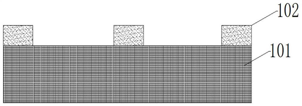
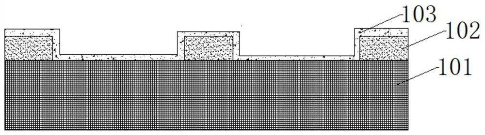
[0038] Such as Figure 1-6 As shown, this embodiment provides a method for heterogeneous integration of a compound semiconductor and a silicon-based complementary metal oxide semiconductor wafer. The compound semiconductor may specifically be an indium phosphide sheet, which includes a compound semiconductor substrate 101 and a compound semiconductor substrate 101 The epitaxial layer 102 deposited on the surface of the bottom 101, the silicon-based complementary metal oxide semiconductor wafer is a silicon-based wafer processed by a CMOS process, including the following steps:

[0039] Selective etching of the compound semiconductor epitaxial layer 102, specifically, etching along the longitudinal and lateral directions of the compound semiconductor epitaxial layer 102 until the surface of the compound semiconductor substrate 101 is exposed, so as to form criss-cross etch grooves on the compound semiconductor ;

[0040] Form a bonding dielectric layer 103 on the etched surfac...

Embodiment 2

[0046] This embodiment provides a method for heterogeneous integration of a compound semiconductor and a silicon-based complementary metal oxide semiconductor wafer. The compound semiconductor may specifically be a gallium arsenide wafer, which includes a compound semiconductor substrate and a compound semiconductor substrate deposited on the surface of the compound semiconductor substrate. The epitaxial layer, the silicon-based complementary metal oxide semiconductor wafer is a silicon-based wafer processed by a CMOS process, including the following steps:

[0047] Selectively etching the compound semiconductor epitaxial layer, specifically, etching along the longitudinal and lateral directions of the compound semiconductor epitaxial layer until the surface of the compound semiconductor substrate is exposed, so as to form criss-cross etch grooves on the compound semiconductor;

[0048] Form a bonding dielectric layer on the etched surface of the epitaxial layer and the inner g...

Embodiment 3

[0054] This embodiment provides a method for heterogeneous integration of a compound semiconductor and a silicon-based complementary metal oxide semiconductor wafer. The compound semiconductor may specifically be a gallium arsenide wafer, which includes a compound semiconductor substrate and a compound semiconductor substrate deposited on the surface of the compound semiconductor substrate. The epitaxial layer, the silicon-based complementary metal oxide semiconductor wafer is a silicon-based wafer processed by a CMOS process, including the following steps:

[0055] Selectively etching the compound semiconductor epitaxial layer, specifically, etching along the longitudinal and lateral directions of the compound semiconductor epitaxial layer until the surface of the compound semiconductor substrate is exposed, so as to form criss-cross etch grooves on the compound semiconductor;

[0056] Form a bonding dielectric layer on the etched surface of the epitaxial layer and the inner g...


PUM

PropertyMeasurementUnit
thicknessaaaaaaaaaa
thicknessaaaaaaaaaa

Abstract

The invention relates to the field of semiconductor materials, in particular to a method for heterogeneous integration of compound semiconductors and silicon-based complementary metal oxide semiconductor wafers, comprising: selectively etching the compound semiconductor epitaxial layer to form an etching groove on the compound semiconductor; Form a bonding dielectric layer on the etching surface of the layer and the inner groove wall of the etching groove; coat a thermosetting adhesive layer on the silicon-based substrate; bond the above-mentioned compound semiconductor and silicon-based complementary metal oxide semiconductor wafers; etch The substrate of the compound semiconductor, forming part of the bonding medium layer and the adhesive layer. The etching groove formed by selective etching in the present invention facilitates the discharge of air bubbles in the thermosetting adhesive layer, forms a bonding medium layer on the compound semiconductor, protects the surface of the compound semiconductor, and through the bonding of the thermosetting adhesive layer and the bonding medium layer, Good bonding of the compound semiconductor epitaxial layer and the silicon-based complementary metal oxide semiconductor wafer is realized.

Description

technical field [0001] The invention relates to the field of semiconductor materials, in particular to a heterogeneous integration method and a heterogeneous integration device of a compound semiconductor and a silicon-based complementary metal oxide semiconductor wafer. Background technique [0002] Modern integrated circuits based on silicon-based CMOS technology continue to improve in terms of integration, power consumption, and device characteristics as the feature size of CMOS devices shrinks. On the other hand, compound semiconductor devices and integrated circuits have made great progress in the fields of ultra-high-speed circuits, microwave circuits, terahertz circuits, and optoelectronic integrated circuits. Since silicon-based semiconductor CMOS chips and compound semiconductor semiconductor chips are difficult to produce in the same fab, process compatibility cannot be achieved. However, if the two are organically combined to break through the limited selection of...

Claims


Application Information

Patent Timeline
Patent Type & Authority Patents(China)
IPC IPC(8): H01L21/762H01L21/8238H01L27/092
CPCH01L21/762H01L21/8238H01L27/0922
Inventor 常虎东孙兵刘洪刚金智
Owner INST OF MICROELECTRONICS CHINESE ACAD OF SCI
Why Eureka
Try Eureka