In-plate electroless nickel-immersion gold classification connecting finger optical module PCB manufacturing method

A production method and golden finger technology, which is applied in the fields of printed circuit manufacturing, coating of non-metallic protective layer, secondary treatment of printed circuit, etc., can solve the problem of falling off of the anti-soldering area of ​​the finished board, so as to reduce the attack and strengthen the bonding force , Reduce the effect of falling off the solder resist part

Inactive Publication Date: 2018-06-29
深圳欣强智创电路板有限公司
View PDF3 Cites 5 Cited by
  • Summary
  • Abstract
  • Description
  • Claims
  • Application Information

AI Technical Summary

Problems solved by technology

[0013] For PCB boards produced by the above method, since the stripping solution is strongly alkaline, after the solder resist, the ink or dry film has been stripped three times. The board has the problem that the welding area falls off

Method used


Image

  • In-plate electroless nickel-immersion gold classification connecting finger optical module PCB manufacturing method

Examples


Embodiment Construction

[0047] In order to make the object, technical solution and advantages of the present invention clearer, the present invention will be further described in detail below in conjunction with the accompanying drawings and embodiments. It should be understood that the specific embodiments described here are only used to explain the present invention, not to limit the present invention.

[0048] To achieve the above object, the technical scheme of the present invention is as follows:

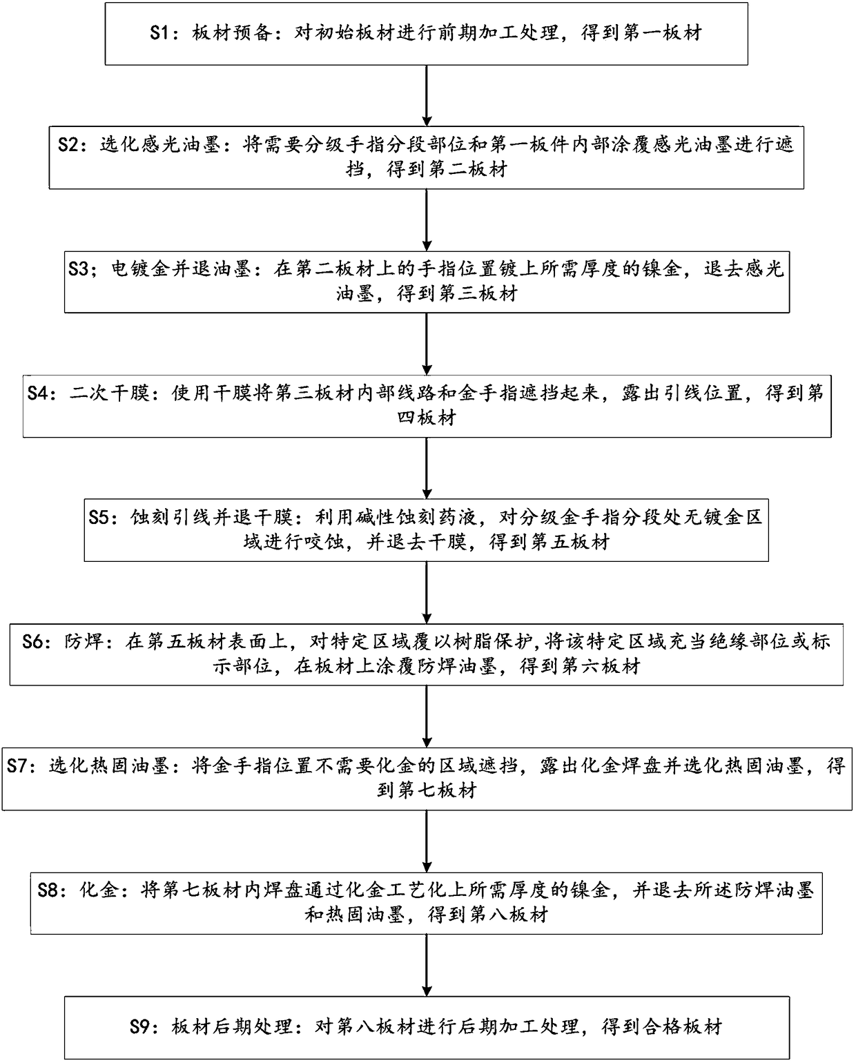
[0049] see figure 1 As shown, in this specific embodiment, the present invention provides a method for manufacturing a gold-finger optical module PCB board with in-board gold classification, and the manufacturing method includes the following steps:

[0050] S1: plate preparation: pre-processing the initial plate to obtain the first plate;

[0051] S2: Selection of photosensitive ink: apply photosensitive ink to the segmented part of the finger to be graded and the inside of the first plate to block...


PUM


Abstract

The invention discloses an in-plate electroless nickel-immersion gold classification connecting finger optical module PCB manufacturing method which comprises steps of plate preparation, partial photosensitive ink treatment, gold electroplating, removing ink, secondary membrane drying, lead etching, dried membrane removal, protection welding, partial thermosetting ink treatment, electroless nickel-immersion gold and later plate treatment. Compared with a conventional common manufacturing process, the method is capable of reducing the cost on the one hand since production procedures are adjusted, that is, the step of protection welding is carried out after the step of lead etching, and thus the three times of membrane removal steps after protection welding are reduced into once; and on theother hand, attack of a strong-alkali eluant to the welding protection ink can be reduced, the bonding force of protection welding parts can be improved, and the problem that protection welding partsof finished plates are peeled off can be reduced.

Description

technical field [0001] The invention belongs to the field of PCB board manufacturing, and in particular relates to a method for manufacturing a PCB of a graded gold finger optical module with gold in the board. Background technique [0002] PCB (Printed Circuit Board), the Chinese name is printed circuit board, also known as printed circuit board, is an important electronic component, a support for electronic components, and a carrier for electrical connections of electronic components. Because it is made using electronic printing, it is called a "printed" circuit board. In recent years, with the rapid development of integrated circuit technology, the demand for PCB boards has been expanding day by day, and the manufacturing technology of PCB boards has also been continuously improved. [0003] In the existing technology, the common PCB board manufacturing steps are as follows: [0004] (1) Make the outer layer: process the gold fingers evenly on the outer layer; [0005]...

Claims


Application Information

Patent Timeline
Patent Type & Authority Applications(China)
IPC IPC(8): H05K3/24H05K3/28
CPCH05K3/243H05K3/282H05K2203/14
Inventor 宋国伟殷大望
Owner 深圳欣强智创电路板有限公司
Why Eureka
Try Eureka