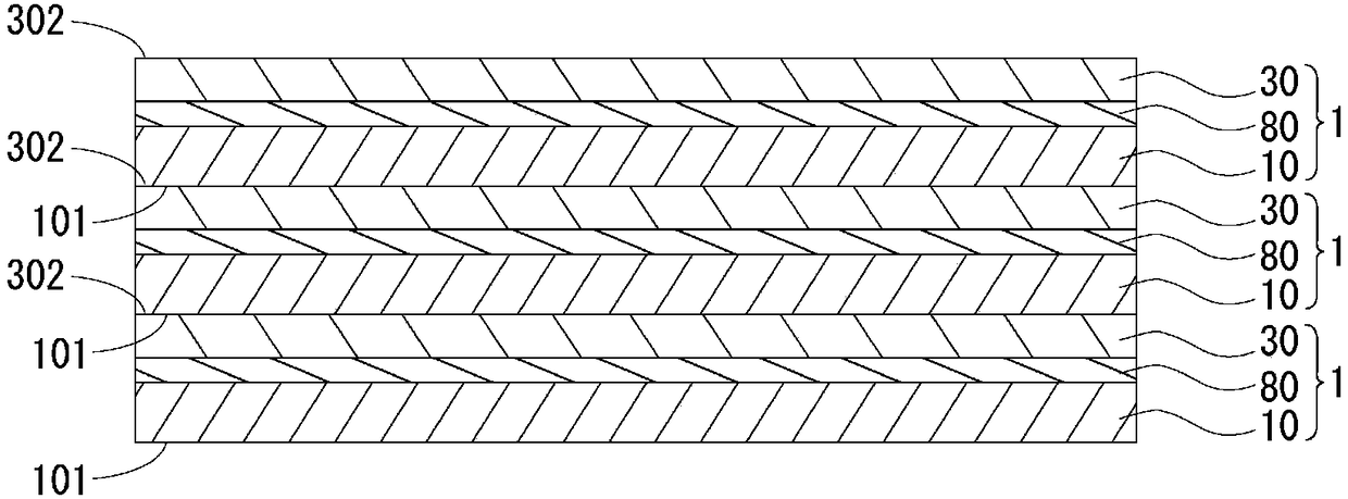
Semiconductor processing sheet
A technology for semiconductors and wafers, which is applied in semiconductor/solid-state device manufacturing, film/sheet release liners, film/sheet adhesives, etc. It can solve problems such as wafer breakage, and achieve not easy adhesion and excellent The effect of light transmission
- Summary
- Abstract
- Description
- Claims
- Application Information
AI Technical Summary
Problems solved by technology
Method used
Image
Examples
Embodiment 1
[0198] (1) Manufacture of base material
[0199] A polyvinyl chloride film was produced as a base material by a calendering film method. The arithmetic mean roughness Ra of the first surface of the polyvinyl chloride film is 0.03 μm, and the tensile elastic modulus (Young's modulus) in the MD direction at 23° C. measured in accordance with JIS K7161:1994 is 250 MPa, and the thickness is 80 μm.
[0200] In addition, the arithmetic mean roughness Ra in this example is obtained by measuring 10 points in the plane according to JIS B061:2013 using a touch-type surface roughness meter ("SURFTEST SV-3000" manufactured by Mitsutoyo Corporation) and calculating the average value. value.
[0201] In addition, with respect to the above substrate alone, the transmittance of laser light for printing (wavelength: 532nm), the transmittance of laser light for stealth dicing (wavelength: 1600nm), and the transmittance of infrared light for inspection (wavelength: 1069nm) were evaluated. , a...
Embodiment 2
[0210] (1) Manufacture of base material
[0211] An ethylene-methacrylic acid copolymer film was produced as a substrate by a T-die film forming method. The arithmetic mean roughness Ra of the first surface of the ethylene-methacrylic acid copolymer film is 0.05 μm, and the tensile modulus of elasticity (Young's modulus) in the MD direction at 23° C. measured in accordance with JIS K7161:1994 It is 130MPa and the thickness is 80μm.
[0212] In addition, with regard to the above substrate alone, the transmittance of laser light for printing (wavelength: 532nm), the transmittance of laser light for stealth dicing (wavelength: 1600nm), and the transmittance of infrared light for inspection (wavelength: 1069nm) were evaluated. , all show excellent transmittance.
[0213] (2) Preparation of Adhesive Composition (II)
[0214] 99 parts by mass of butyl acrylate and 1 part by mass of acrylic acid were copolymerized to obtain an acrylic copolymer having a weight average molecular we...
Embodiment 3
[0219] (1) Manufacture of base material
[0220] An ethylene-vinyl acetate copolymer film was produced as a base material by a T-die film forming method. The arithmetic mean roughness Ra of the first surface of the ethylene-vinyl acetate copolymer film is 0.06 μm, and the tensile modulus of elasticity (Young's modulus) in the MD direction at 23° C. measured in accordance with JIS K7161:1994 It is 75MPa and the thickness is 100μm.
[0221] In addition, with respect to the above substrate alone, the transmittance of laser light for printing (wavelength: 532nm), the transmittance of laser light for stealth dicing (wavelength: 1600nm), and the transmittance of infrared light for inspection (wavelength: 1069nm) were evaluated. , all show excellent transmittance.
[0222] (2) Preparation of Adhesive Composition (III)
[0223] An acrylic copolymer having a weight average molecular weight of 420,000 was obtained by copolymerizing 40 parts by mass of 2-ethylhexyl acrylate, 40 parts ...
PUM
| Property | Measurement | Unit |
|---|---|---|
| Arithmetic mean roughness | aaaaa | aaaaa |
| Tensile modulus of elasticity | aaaaa | aaaaa |
| Thickness | aaaaa | aaaaa |
Abstract
Description
Claims
Application Information


