Silicon-based photonic integrated structure and preparation method

A photonic integration, silicon-based technology, applied in the direction of light guide, optics, optical components, etc., can solve the problems of low communication signal transmission efficiency, complex assembly process, high cost of optical components, improve signal transmission quality, facilitate small size, The effect of reducing the difficulty of packaging

Active Publication Date: 2018-07-10
WUHAN TELECOMM DEVICES
View PDF6 Cites 6 Cited by
  • Summary
  • Abstract
  • Description
  • Claims
  • Application Information

AI Technical Summary

Problems solved by technology

[0004] The technical problem to be solved by the present invention is: with the increasing demand for communication in modern life, in the existing optical components, the internal components are built using discrete components, resulting in low transmission efficiency of communication signals and high cost of optical components , large volume, high power consumption, and complex assembly process are becoming more and more serious

Method used


Image

  • Silicon-based photonic integrated structure and preparation method
  • Silicon-based photonic integrated structure and preparation method
  • Silicon-based photonic integrated structure and preparation method

Examples


Embodiment 1

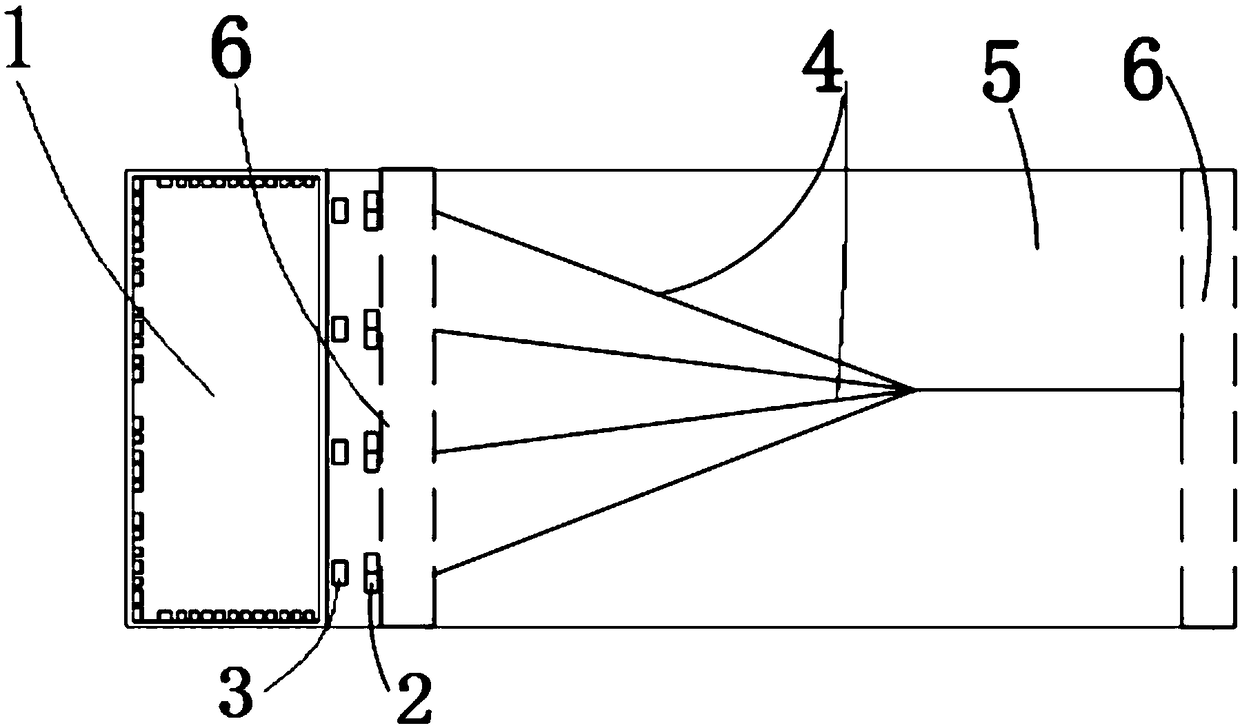
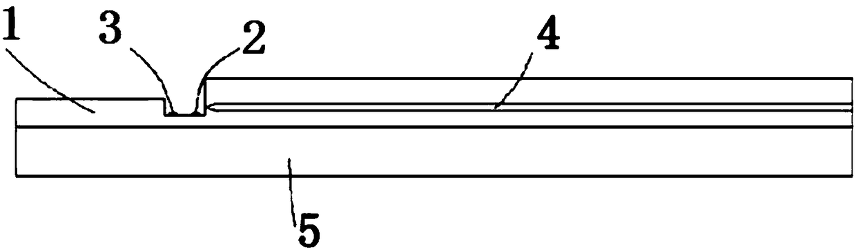
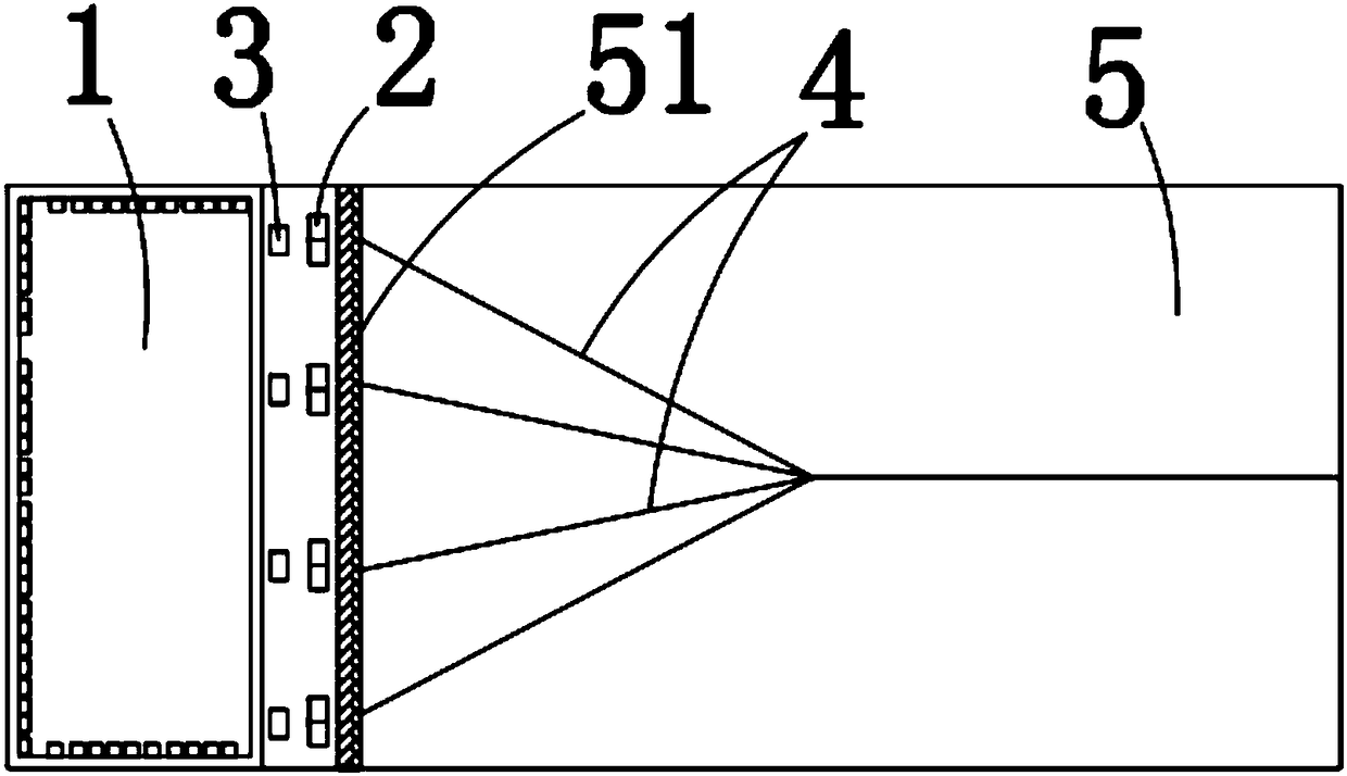
[0036] Such as Figure 1 ~ Figure 2 As shown, the present invention provides a silicon-based photonic integrated structure, which includes: a laser drive circuit 1, at least one laser 2, a number of monitoring detectors 3 corresponding to the laser 2, an optical waveguide 4 and a silicon-based substrate 5 The laser drive circuit 1 is electrically connected to the laser 2; the laser 2, the monitoring detector 3 and the optical waveguide 4 are optically connected; the laser drive circuit 1, the laser 2, the monitoring detector 3 and the optical waveguide 4 are all set on the same silicon-based substrate 5. During operation, the laser driving circuit 1 drives the laser 2 to generate light waves, and after the light waves pass through the optical waveguide 4, they enter other subsequent matched components in the direction of the optical path.

[0037] In this embodiment, laser drive circuit 1, laser 2 components, and multi-optical path composite components are integrated on a sil...

Embodiment 2

[0044] On the basis of Embodiment 1 above, and based on the common inventive concept, this embodiment provides a light emitting component and a light receiving component including the above silicon-based photonic integrated structure. The light-emitting component proposed in the embodiment of the present invention can be realized by using the silicon-based photonic integrated structure as described in Embodiment 1, or can be realized by an expansion scheme based on the silicon-based photonic integrated structure in the above-mentioned embodiment 1. Therefore, although some structures with the same name have different labels, it is mainly to facilitate the description of different embodiments.

[0045] combine Figure 7 ~ Figure 8 As shown, a silicon-based photonic integrated optical emission module, the emission module includes: a tube shell 7, a multilayer ceramic 8, a laser drive circuit 9, a laser 10, a wavelength division multiplexer 11, a silicon-based substrate 12 and a ...


PUM


Abstract

The present invention belongs to the semiconductor optoelectronic technological field and relates to a silicon-based photonic integrated structure and a preparation method. The integrated structure comprises a laser driving circuit, at least one laser, monitoring detectors, an optical waveguide, and a silicon-based substrate, wherein the number of the at least one laser is corresponding to the number of the monitoring detectors; the laser driving circuit is electrically connected with the lasers; the lasers, the monitoring detectors, and the optical waveguides are optically connected with oneanother; and the laser driving circuit, the lasers, the monitoring detectors, and the optical waveguide are all disposed on the same silicon-based substrate. According to the silicon-based photonic integrated structure of the invention, the laser driving circuit, a multi-wavelength chip and a multi-optical path composite chip are integrated on the same substrate, and therefore, the silicon-based photonic integrated structure has the advantages of high integration, high performance, low cost and easiness in packaging. With the silicon-based photonic integrated structure adopted, the further development of a communication module in the corresponding industry in high integration and miniaturization can be benefitted.

Description

【Technical field】 [0001] The invention relates to the technical field of semiconductor optoelectronics, in particular to a silicon-based photonic integrated structure and a preparation method. 【Background technique】 [0002] With the rapid development of modern scientific information technology and communication networks, people have higher and higher demands for communication, and produce high-speed, large-bandwidth, high-integration, low-power, low-cost, and easy-to-package devices that meet the needs of use. All kinds of communication equipment modules have become the core development direction of this industry. [0003] In the currently used optical devices, the materials used for hybrid integration are usually multiple isolated semiconductor substrates, and often contain materials of different systems, such as III-V semiconductor materials, ferroelectric materials, organic polymers, liquid crystals, etc. These chips with different functions and different materials are ...

Claims


Application Information

Patent Timeline
Patent Type & Authority Applications(China)
IPC IPC(8): G02B6/42
CPCG02B6/4204G02B6/4244G02B6/4245
Inventor 郭浩荣徐红春刘成刚宋小平岳阳阳
Owner WUHAN TELECOMM DEVICES
Why Eureka
Try Eureka