Ultraviolet light emitting diode and manufacturing method thereof
A technology for light-emitting diodes and a manufacturing method, which is applied to semiconductor devices, electrical components, circuits, etc., can solve problems such as warping of ultraviolet light-emitting diodes, and achieve the improvement of light-emitting wavelength uniformity, improvement of surface temperature uniformity, and reduction of warpage. Effect
- Summary
- Abstract
- Description
- Claims
- Application Information
AI Technical Summary
Problems solved by technology
Method used
Image

Examples
Embodiment 1
[0051] like Figure 5 ~ Figure 11 As shown, the present embodiment provides a method for manufacturing an ultraviolet light-emitting diode, comprising steps:
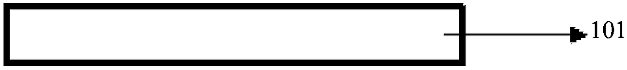
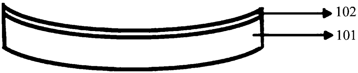
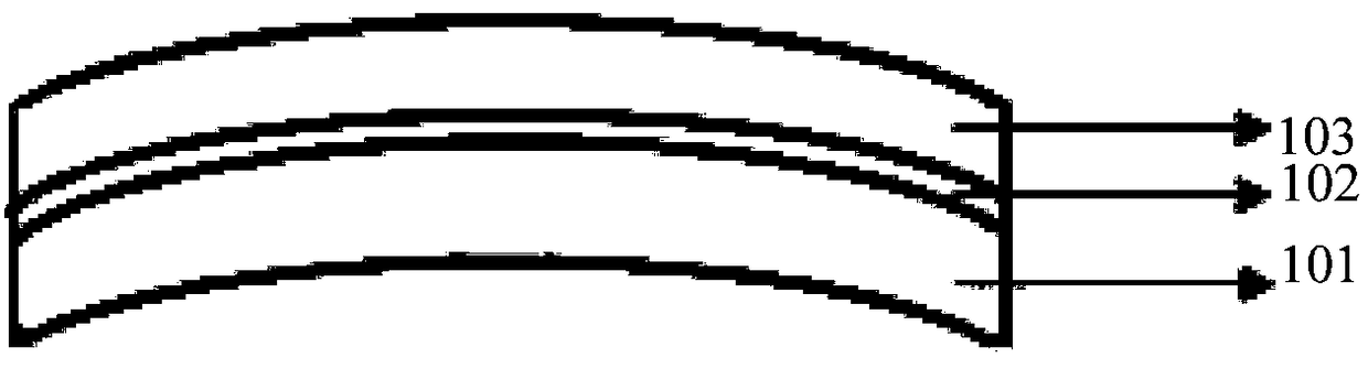
[0052] like Figure 5 ~ Figure 7As shown, step 1) S11 is firstly performed to provide a substrate 201, and a buffer layer 202 and an n-type layer 203 are formed on the substrate 201, and the buffer layer 202 and the n-type layer 203 have warpage.
[0053] In this embodiment, the substrate 201 is a sapphire substrate, and the sapphire substrate can be a flat sapphire substrate or a patterned sapphire substrate. Of course, other types of substrates can also be selected according to different requirements. Such as Si substrate, SiC substrate, GaN substrate, etc., and are not limited to the examples listed here.
[0054] In the MOCVD epitaxial equipment, the chemical vapor deposition process is used to deposit the buffer layer 202 on the substrate 201. The material of the buffer layer 202 can be AlN, etc. At this time, th...
Embodiment 2
[0083] This embodiment provides an ultraviolet light emitting diode, the basic structure of which is the same as that of embodiment 1, wherein the difference from embodiment 1 is that the stress modulation layer 204 is located in the n-type layer 203 .
Embodiment 3
[0085] This embodiment provides an ultraviolet light emitting diode, the basic structure of which is the same as that of embodiment 1, wherein the difference from embodiment 1 is that the stress modulation layer 204 is located in the quantum well light emitting layer 205 .
[0086] As mentioned above, the ultraviolet light-emitting diode and its manufacturing method of the present invention have the following beneficial effects:
[0087] The present invention is aimed at ultraviolet light-emitting diodes, especially deep ultraviolet light-emitting diodes, introducing Al between the n-type layer 203 of the epitaxial structure and the quantum well light-emitting layer 205 x Ga y In 1-x-y In the N stress modulation layer 204, the Al component is adjusted to more than 70%, which can reduce the warping of the subsequent growth of the quantum well light-emitting layer, and at the same time improve the surface temperature uniformity of the quantum well light-emitting layer, thereby ...
PUM
| Property | Measurement | Unit |
|---|---|---|
| Doping concentration | aaaaa | aaaaa |
| Luminous wavelength | aaaaa | aaaaa |
Abstract
Description
Claims
Application Information