Supercharge Your Innovation With Domain-Expert AI Agents!

High-quality semiconductor epitaxial wafer and preparation method thereof

A semiconductor, high-quality technology, applied in semiconductor/solid-state device manufacturing, semiconductor devices, electrical components, etc., to achieve the effects of improving leakage performance and luminous efficiency, improving uniformity of luminous wavelength, and precise and controllable thickness

Pending Publication Date: 2022-03-04
JIANGSU INST OF ADVANCED SEMICON CO LTD
View PDF0 Cites 3 Cited by
  • Summary
  • Abstract
  • Description
  • Claims
  • Application Information

AI Technical Summary

Problems solved by technology

[0003] The main purpose of the present invention is to propose a high-quality semiconductor epitaxial wafer and its preparation method based on the current semiconductor material heterogeneous growth epitaxial defect problem, to overcome the deficiencies in the prior art

Method used


Image

  • High-quality semiconductor epitaxial wafer and preparation method thereof
  • High-quality semiconductor epitaxial wafer and preparation method thereof
  • High-quality semiconductor epitaxial wafer and preparation method thereof

Examples


preparation example Construction

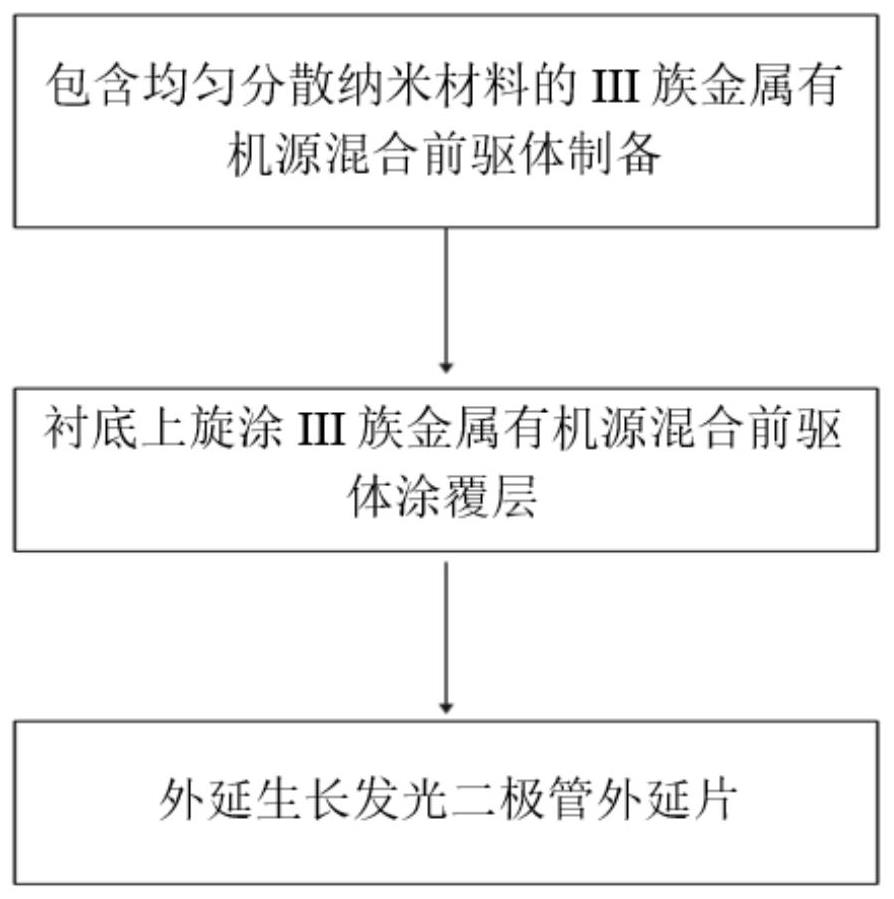
[0028] Another aspect of the embodiments of the present invention provides a method for preparing a high-quality semiconductor epitaxial wafer comprising:

[0029] Provide Group III metal-organic source hybrid precursors containing uniformly dispersed nanomaterials;

[0030] Coating the Group III metal-organic source mixed precursor on the substrate to obtain the Group III metal-organic source mixed precursor coating layer, and then placing the substrate with the Group III metal-organic source mixed precursor coating layer on In the MOCVD reaction chamber, the metal-organic source of group III is introduced, and annealing and recrystallization are carried out in the mixed atmosphere of group V element source and reducing gas, so as to form uniformly distributed nanomaterials and nano-growth structures of group III-V compounds, and obtain Stress relief buffer layer;

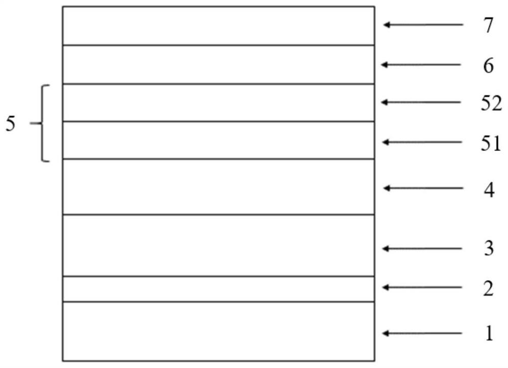
[0031] A semiconductor epitaxial structure is grown on the stress release buffer layer to produce a high-quali...

Embodiment 1

[0094] 1) Preparation of Ni nanoparticle dispersion

[0095] Using absolute ethanol, add 30% by mass fraction of nano-Ni powder with a diameter of 30 to 80 nm, add 0.15% by mass fraction of citric acid dispersant, and sonicate for 2 hours at room temperature;

[0096] 2) Preparation of Ni nanoparticles TMG source

[0097] The Ni nanoparticles were separated from the solvent, quickly dried and immediately mixed with a high-purity TMG source. The mass fraction of Ni nanoparticles was 40%, and ultrasonicated at 40°C for 60 minutes to obtain a TMG source mixed precursor with uniformly dispersed Ni nanoparticles;

[0098] 3) Spin coating Ni nanoparticles TMG source mixed precursor

[0099] In the glove box N 2 In the atmosphere, the Ni nanoparticle TMG source mixed precursor is spin-coated on the sapphire substrate at a speed of 4000rpm by the spin coating method of the homogenizer, and the TMG source mixed precursor with a thickness of 30nm uniformly dispersed Ni nanoparticles i...

Embodiment 2

[0108] 1) Preparation of Ni nanoparticle dispersion

[0109] Using absolute ethanol, add 30% by mass fraction of nano-Ni powder with a diameter of 30 to 80 nm, add 0.15% by mass fraction of citric acid dispersant, and sonicate for 2 hours at room temperature;

[0110] 2) Preparation of Ni nanoparticles TMG source

[0111] The Ni nanoparticles were separated from the solvent, quickly dried and immediately mixed with a high-purity TMG source. The mass fraction of Ni nanoparticles was 40%, and ultrasonicated at 40°C for 60 minutes to obtain a TMG source mixed precursor with uniformly dispersed Ni nanoparticles;

[0112] 3) Spin coating Ni nanoparticles TMG source mixed precursor

[0113] In the glove box N 2 In the atmosphere, the Ni nanoparticle TMG source mixed precursor is spin-coated on the sapphire substrate at a speed of 4000rpm by the spin coating method of the homogenizer, and the TMG source mixed precursor with a thickness of 800nm ​​uniformly dispersed Ni nanoparticle...


PUM

PropertyMeasurementUnit
diameteraaaaaaaaaa
thicknessaaaaaaaaaa
thicknessaaaaaaaaaa

Abstract

The invention discloses a high-quality semiconductor epitaxial wafer and a preparation method thereof. The preparation method comprises the following steps: providing a group III metal organic source mixed precursor containing a uniformly dispersed nano material, coating the group III metal organic source mixed precursor on a substrate to obtain a group III metal organic source mixed precursor coating layer, and then performing annealing recrystallization to obtain a stress release buffer layer; and growing to form a semiconductor epitaxial structure to prepare a high-quality semiconductor epitaxial wafer. The metal organic source coating layer is prepared on the substrate, and the MOCVD reaction cavity annealing recrystallization and the nanometer material dispersed metal organic source coating layer are combined to gradually form two crystal nucleus distributions to provide a nucleation center, the epitaxial layer stress is gradually released, the lateral epitaxial growth is enhanced, the epitaxial layer dislocation density extension is inhibited, and the defect density is reduced. The growth quality of a quantum well light-emitting layer is improved, the electric leakage performance and the light-emitting efficiency are improved, meanwhile, the light-emitting wavelength uniformity is improved, and the requirement for the epitaxial uniformity of a Micro-LED can be met.

Description

technical field [0001] The invention relates to a high-quality semiconductor epitaxial wafer and a preparation method thereof, belonging to the technical field of semiconductor material epitaxy. Background technique [0002] III-V compound semiconductor materials have been widely used in optoelectronic devices, optoelectronic integration, ultra-high-speed microelectronic devices, ultra-high frequency microwave devices and circuits, and have broad prospects. Since III-nitrides are generally heteroepitaxy on heterogeneous substrates such as sapphire or SiC, the lattice constant and thermal mismatch between different materials will generate dislocations or defects, which extend upward with the growth of the epitaxial layer , these dislocations behave as non-radiative recombination centers when the device is working, which affects the efficiency of the device. At the same time, as a leakage channel, the leakage current increases and the device ages rapidly, affecting the working...

Claims


Application Information

Patent Timeline
Patent Type & Authority Applications(China)
IPC IPC(8): H01L21/205H01L33/00H01L33/12B82Y10/00B82Y30/00B82Y40/00
CPCH01L21/0254H01L21/02458H01L21/0262H01L33/0075H01L33/12H01L21/02658B82Y30/00B82Y40/00B82Y10/00
Inventor 闫其昂王国斌
Owner JIANGSU INST OF ADVANCED SEMICON CO LTD
Features
  • R&D
  • Intellectual Property
  • Life Sciences
  • Materials
  • Tech Scout
  • Unparalleled Data Quality
  • Higher Quality Content
  • 60% Fewer Hallucinations
Learn More