A method for wet process of thin film transistor array substrate

A technology of thin film transistors and array substrates, which is applied in the field of wet process of thin film transistor array substrates, can solve the problems of adverse effects on the performance and reliability of TFT devices, the easy diffusion adhesion of metal Cu, and the increase of Cu etching rate. Effects of chemical reaction, simplification of subsequent treatment process, and performance improvement

Active Publication Date: 2021-01-05
TCL CHINA STAR OPTOELECTRONICS TECH CO LTD
View PDF8 Cites 0 Cited by
  • Summary
  • Abstract
  • Description
  • Claims
  • Application Information

AI Technical Summary

Problems solved by technology

[0004] However, due to the characteristics of easy diffusion and poor adhesion of metallic Cu, a barrier layer is generally used in the Cu process to prevent Cu from diffusing and increase its adhesion.
In the process of wet etching, due to the difference in activity between Cu and the metal (such as Mo) of the barrier layer, electrochemical reactions are prone to occur, resulting in an increase in the etching rate of Cu, which in turn leads to the phenomenon that the underlying Cu is hollowed out.
As a result, it will adversely affect the performance and reliability of TFT devices

Method used


Image

  • A method for wet process of thin film transistor array substrate
  • A method for wet process of thin film transistor array substrate
  • A method for wet process of thin film transistor array substrate

Examples


Embodiment Construction

[0027] Embodiments of the invention will now be described more fully with reference to the accompanying drawings, in which exemplary embodiments of the invention are shown. However, this invention may be embodied in many different forms and should not be construed as limited to the embodiments set forth herein; rather, these embodiments are provided so that this disclosure will be thorough and complete, and will provide Those of ordinary skill in the art fully convey the concept of the embodiments of the present invention. In the following detailed description, numerous specific details are set forth by way of example in order to provide a thorough understanding of the relevant teachings.

[0028] A method for wet processing of a thin film transistor array substrate according to the concept of the present invention will be described in detail below with reference to the accompanying drawings.
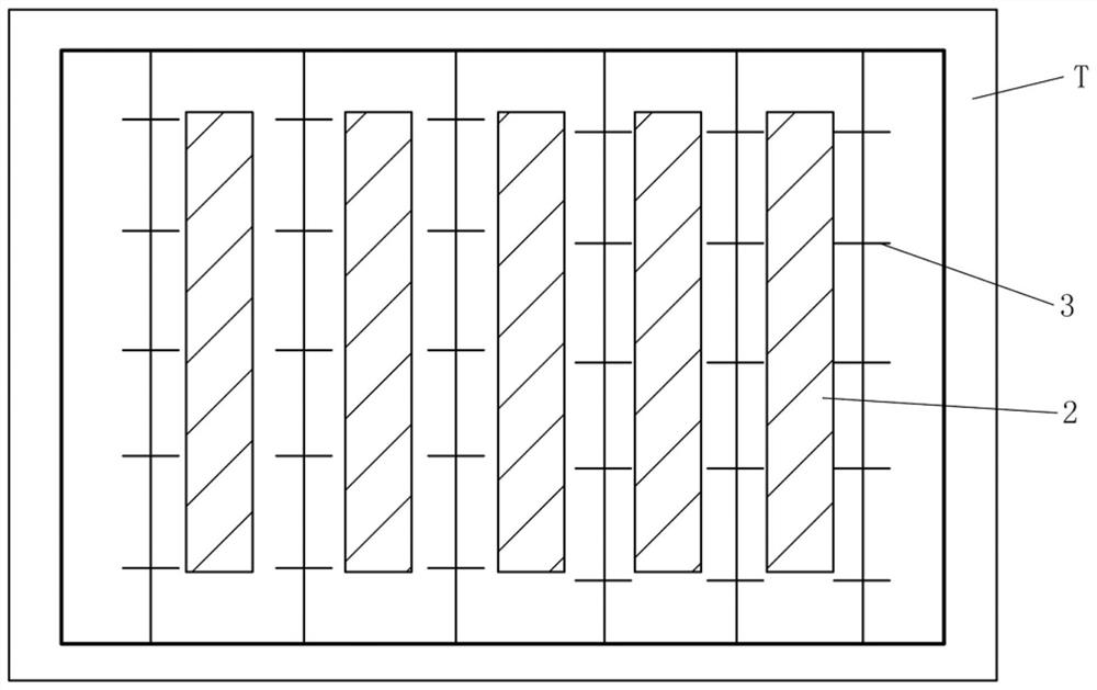
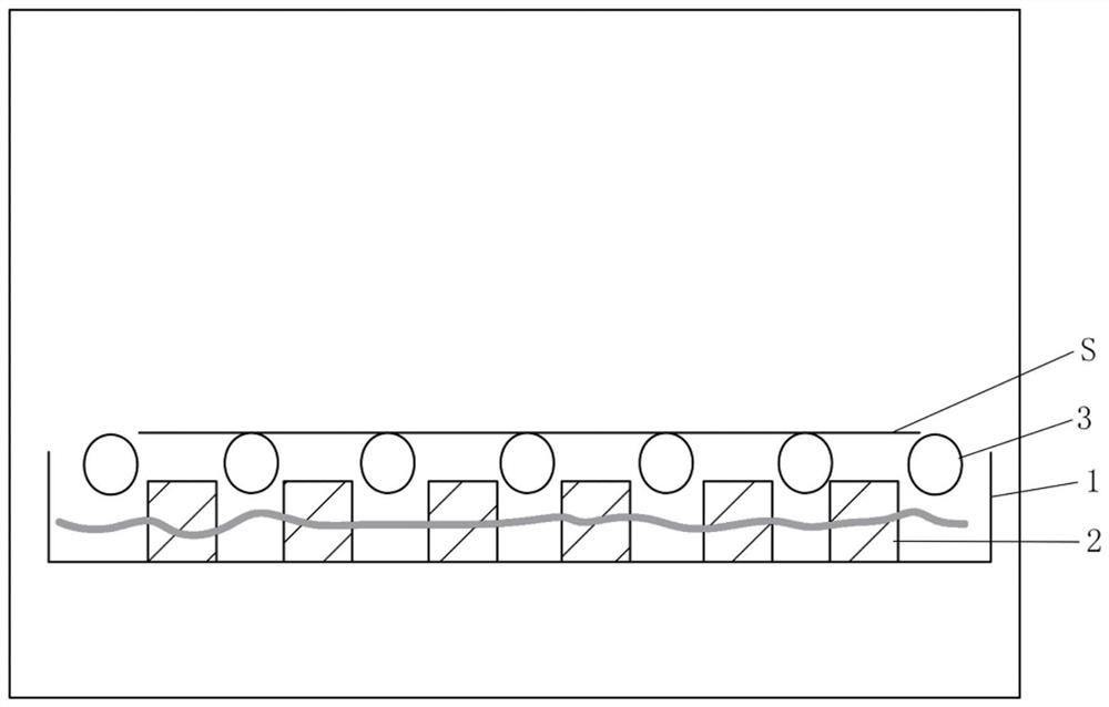
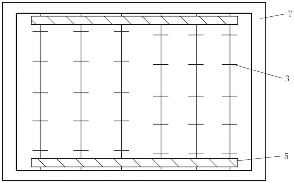
[0029] The general idea of ​​the present invention is: by adding a metal piece wit...


PUM


Abstract

The invention provides a method for a wet process of a thin film transistor array substrate. The method comprises the step of placing a substrate in a processing room so that a metal layer and a blocking layer both are in contact with a medium liquid in the processing room for wet processing, wherein the metal layer and the blocking layer are formed on the substrate, the blocking layer is arrangedon the metal layer, a metal piece of which electrochemical activity is larger than that of the metal layer and which is not in chemical reaction with the medium liquid is arranged in the processing room, and the metal layer does not generate electrochemical reaction with the medium liquid. By the method, an electrochemical corrosion phenomenon occurring in the fabrication process of the thin filmtransistor array substrate can be prevented, and the quality of the thin film transistor array substrate is improved.

Description

technical field [0001] The invention belongs to the field of display technology, and more specifically, relates to a wet process method for a thin film transistor array substrate. Background technique [0002] TFT-LCD (Thin Film Transistor Liquid Crystal Display) is widely used in industries such as computers, video terminals, communications and instrumentation due to its low power consumption and fast response speed. For example, it is mainly used in notebook computers, desktop computer monitors, Industrial monitors, global satellite positioning systems (GPS), personal digital assistants (PDAs), game consoles, videophones, portable VCDs, DVDs and other portable devices. After continuous development and innovation, TFT-LCD has rapidly grown into a mainstream display. [0003] With people's pursuit of large size, high resolution LCD and low cost, it is imperative to invest in large size glass equipment. In order to overcome the problems of large-size glass wiring and RC del...

Claims


Application Information

Patent Timeline
Patent Type & Authority Patents(China)
IPC IPC(8): H01L27/12G02F1/1333
CPCG02F1/1333H01L27/124H01L27/127
Inventor 蔡良毅
Owner TCL CHINA STAR OPTOELECTRONICS TECH CO LTD
Why Eureka
Try Eureka