Semiconductor device and method for manufacturing semiconductor device

A semiconductor and substrate technology, applied in semiconductor devices, electrical components, circuits, etc., can solve problems such as breakdown and failure to maintain withstand voltage

Active Publication Date: 2021-04-27
SHINDENGEN ELECTRIC MFG CO LTD
View PDF7 Cites 0 Cited by
  • Summary
  • Abstract
  • Description
  • Claims
  • Application Information

AI Technical Summary

Problems solved by technology

In this case, after a negative potential is applied to the above-mentioned second electrode 724, the depletion layer extending from the pn junction surface between the second semiconductor layer 714 and the third semiconductor layer 716 to the second electrode 724 side may be depleted. Contact with the metal inside the above-mentioned cavity S results in breakdown (breakdown) in the reach through mode, so that the withstand voltage can no longer be maintained (refer to Figure 23 The area surrounded by dotted line A)
[0011] Furthermore, such problems not only occur in MOSFETs, but also occur in diodes and IGBTs, etc.
In addition, such a problem does not only occur when the trench of the n-type semiconductor layer is backfilled with a p-type epitaxial layer, but also occurs when the trench of the p-type semiconductor layer is backfilled with an n-type epitaxial layer.

Method used


Image

  • Semiconductor device and method for manufacturing semiconductor device
  • Semiconductor device and method for manufacturing semiconductor device
  • Semiconductor device and method for manufacturing semiconductor device

Examples


Embodiment approach 1

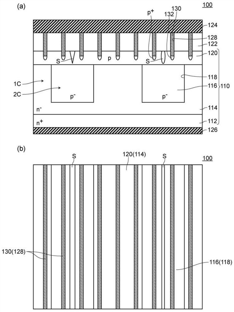
[0067] 1. Configuration of the semiconductor device 100 according to the first embodiment

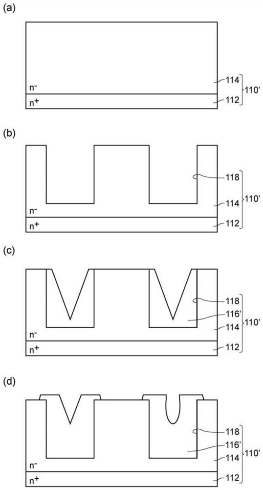
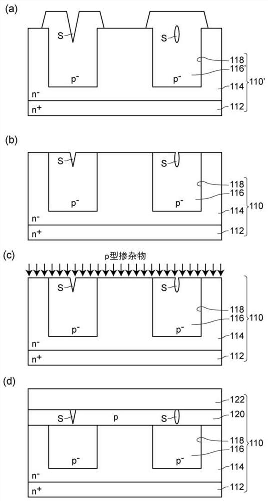
[0068] The semiconductor device 100 according to Embodiment 1 is, for example, figure 1 As shown, it includes: a semiconductor substrate 110 (the same structure as the semiconductor substrate 710, refer to Figure 22 ), at n + Type first semiconductor layer 112 is stacked with n - type second semiconductor layer 114, and the n - The surface of the second semiconductor layer 114 is formed with a plurality of grooves 118 of a predetermined depth arranged in a predetermined direction, and p - type third semiconductor layer 116; the first electrode 126 is located on the surface of the first semiconductor layer 112; the interlayer insulating film 122 is located on the surfaces of the second semiconductor layer 114 and the third semiconductor layer 116, and has: See the prescribed opening 128 formed at least in the region where the third semiconductor layer 116 is formed; the second elec...

Embodiment approach 2

[0114] The semiconductor device 102 according to the second embodiment basically has the same configuration as the semiconductor device 100 according to the first embodiment, but differs from the semiconductor device 100 according to the first embodiment in that the second electrode is directly connected to the third semiconductor layer. . That is, in the semiconductor device 102 according to the second embodiment, as Figure 7 As shown, the inside of the opening 128 is directly filled with the metal constituting the second electrode 124 , and the second electrode 124 is directly connected to the fourth semiconductor layer 120 . In addition, no barrier metal (not shown) is formed on the inner surface of the opening 128 .

[0115] The opening 128 is formed in the entire area except the central portion of the third semiconductor layer as viewed in plan.

[0116] The method of manufacturing a semiconductor device according to the second embodiment basically has the same configu...

Embodiment approach 3

[0122] The semiconductor device 104 according to the third embodiment basically has the same configuration as the semiconductor device 100 according to the first embodiment, but differs from the semiconductor device 104 according to the first embodiment in that it is not a PIN diode but a Schottky barrier diode. device 100. That is, in the semiconductor device 104 according to the third embodiment, as Figure 8 As shown, the metal plug 130 is a barrier metal, and the second electrode 124 is a Schottky barrier diode connected not only to the third semiconductor layer 116 but also to the second semiconductor layer 114 . Furthermore, in the third embodiment, the p + type high-concentration diffusion region 132 . In addition, on the surface of the third semiconductor layer 116, a p-type diffusion region 120' is formed.

[0123] In the semiconductor device 104 according to the third embodiment, the second semiconductor layer 114 on the portion to be sandwiched by the adjacent tr...


PUM

PropertyMeasurementUnit
lengthaaaaaaaaaa
thicknessaaaaaaaaaa
thicknessaaaaaaaaaa

Abstract

The power semiconductor device 100 of the present invention includes: a semiconductor substrate 110, a second semiconductor layer 114 is stacked on the first semiconductor layer 112, a groove 118 is formed on the surface of the second semiconductor layer 114, and a groove 118 is formed in the groove 118. The third semiconductor layer 116 composed of an epitaxial layer; the first electrode 126; the interlayer insulating film 122 having a prescribed opening 128; and the second electrode 124, wherein the inside of the opening 128 is filled with metal and the opening 128 is located away At the central portion of the third semiconductor layer 116 , the second electrode 124 is connected to the third semiconductor layer 116 via a metal, and the surface of the central portion of the third semiconductor layer 116 is covered with an interlayer insulating film 122 . According to the semiconductor device of the present invention, there is provided a semiconductor device including the third semiconductor layer 116 formed of an epitaxial layer formed in the trench 118 and a semiconductor device that is less prone to drop in withstand voltage due to breakdown in punch-through mode.

Description

technical field [0001] The present invention relates to a semiconductor device and a method of manufacturing the semiconductor device. Background technique [0002] Conventionally, a MOSFET having a semiconductor base having a trench of a predetermined depth formed on the surface of an n-type semiconductor layer and a p-type semiconductor layer composed of an epitaxial layer formed in the trench has been widely known (for example, refer to Patent Document 1). [0003] Previous MOSFET700 such as Figure 21 shown, including: a semiconductor substrate 710, the n + Type first semiconductor layer 712 is stacked with n - type second semiconductor layer 714, on the surface of the second semiconductor layer 714, a plurality of grooves 718 of a predetermined depth arranged in a predetermined direction are formed, and p - type third semiconductor layer 716 (refer to Figure 22 In the semiconductor base 710'), wherein, a p-type base layer 720 is formed on a part of the surface of t...

Claims


Application Information

Patent Timeline
Patent Type & Authority Patents(China)
IPC IPC(8): H01L29/78H01L29/41H01L29/739H01L29/861H01L29/868H01L29/872
CPCH01L29/0619H01L29/0634H01L29/0649H01L29/0653H01L29/0692H01L29/0696H01L29/417H01L29/66136H01L29/66143H01L29/66712H01L29/66734H01L29/7395H01L29/7397H01L29/7802H01L29/7813H01L29/861H01L29/872H01L29/78H01L29/868
Inventor 北田瑞枝浅田毅山口武司铃木教章新井大辅
Owner SHINDENGEN ELECTRIC MFG CO LTD
Why Eureka
Try Eureka