Slope control circuit for erasing and writing voltage of non-volatile memory and non-volatile memory
A non-volatile memory and control circuit technology, applied in the field of electronics, can solve problems such as damage and failure of memory cells, and achieve the effect of improving efficiency
- Summary
- Abstract
- Description
- Claims
- Application Information
AI Technical Summary
Problems solved by technology
Method used
Image
Examples
Embodiment 1
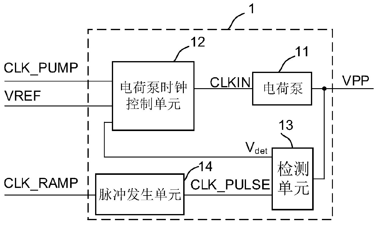
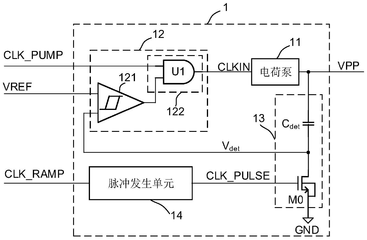
[0041] Such as figure 2 As shown, the slope control circuit of the non-volatile memory erasing voltage involved in this embodiment, the slope control circuit 1 includes a charge pump 11, a charge pump clock control unit 12 and a detection unit 13, and the charge pump 11 is used to generate a target voltage VPP, the detection unit 13 is used to generate the detection voltage V from the target voltage VPP according to the received pulse clock signal CLK_PULSE det , the charge pump clock control unit 12 is used to detect the voltage V det Compared with the reference voltage VREF, the received charge pump clock signal CLK_PUMP is output to the clock input terminal CLKIN of the charge pump 11 according to the comparison result.
[0042] In specific implementation, the pulse clock signal CLK_PULSE is preferably a narrow pulse signal. Since the slope clock signal CLK_RAMP is generally a clock signal similar to a square wave, the pulse generating unit 14 can be used to generate the ...
Embodiment 2
[0057] Such as Figure 9 As shown, the nonvolatile memory involved in this embodiment includes the storage unit 2 and the slope control circuit 1 described in Embodiment 1, the output terminal of the charge pump 11 is electrically connected to the storage unit 2, and the target voltage VPP is used as the storage unit Erase and write voltage of cell 2. Here, the storage unit 2 is equivalent to the load capacitance C of the slope control circuit 1 load .
[0058] Thus, at power-up, the sense voltage V det The initial voltage is zero level, the output of the comparator 121 enables the first AND gate U1, so that the charge pump clock signal CLK_PUMP is output to the clock input terminal CLKIN of the charge pump 11, the charge pump 11 starts, the target voltage VPP rises, and passes the detection Capacitance C det making the detection voltage V det Follow the target voltage VPP to rise; when the detection voltage V det When rising to the reference voltage VREF, the output of th...
PUM
 Abstract
Description
Claims
Application Information


