MEMS pressure sensor based on phase detection principle and preparation method thereof
A pressure sensor and phase detection technology, which is used in fluid pressure measurement, force measurement, piezoelectric device/electrostrictive device, etc. using capacitance change. Advanced problems, to achieve the effect of saving chip area, low price, and improving integration
- Summary
- Abstract
- Description
- Claims
- Application Information
AI Technical Summary
Problems solved by technology
Method used
Image
Examples
Embodiment 1
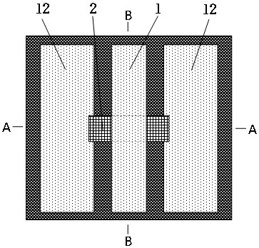
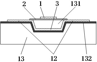
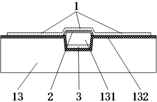
[0031] This embodiment provides a MEMS pressure sensor based on the principle of phase detection, such as Figure 1 ~ Figure 3 As shown, it includes: CPW transmission line, substrate 13, groove 131, buffer medium layer 132, MEMS film 2 and MEMS beam 3; the CPW transmission line is arranged on the substrate 13, and the substrate 13 is provided with concave Groove 131, the MEMS beam 3 is arranged in the groove 131; the MEMS film 2 and the groove 131 form a closed cavity, and the substrate 13 is made of high-resistance silicon with a resistivity greater than 1 kΩ·cm.
[0032] The CPW transmission line includes a CPW signal line 1 located in the middle of the substrate 13 and two CPW ground lines 12 located on both sides of the CPW signal line 1, the CPW signal line 1 and the CPW ground line 12 parallel to each other.
[0033] The groove 131 is located directly below the middle portion of the CPW signal line 1 . The groove 131 is a U-shaped groove, and the axis of the groove 131...
Embodiment 2
[0038] The present invention also provides the preparation method of the above MEMS pressure sensor based on the phase detection principle, such as Figure 5-11 shown, including the following steps:
[0039] S10 prepares the Si substrate 13, the substrate is for example made of high-resistance silicon, its resistivity is greater than 1kΩ·cm, and a groove 131 is etched on the substrate, the depth of the groove is for example 1-50 μm, and then A layer of buffer dielectric layer 132 is grown on the substrate by thermal oxidation, such as Figure 6 shown.
[0040] S20 sequentially pass photolithography, evaporation, and stripping on the buffer medium layer to obtain MEMS beams and CPW ground wires; as Figure 7 As shown; wherein, the MEMS beam 3 and the CPW ground wire 12 are prepared from the same material in the same process step, and are connected to each other.
[0041] S30 deposits and photoetches the PSG sacrificial layer, retains the PSG sacrificial layer inside the groo...
PUM
| Property | Measurement | Unit |
|---|---|---|
| electrical resistivity | aaaaa | aaaaa |
| depth | aaaaa | aaaaa |
| thickness | aaaaa | aaaaa |
Abstract
Description
Claims
Application Information


