Nitride semiconductor light emitting device and manufacturing method thereof

A technology of nitride semiconductors and light-emitting devices, which is applied to the structure of semiconductor devices, semiconductor lasers, and optical waveguide semiconductors. It can solve problems such as easy contamination, affecting device performance and life, and large device resistance. Achieve stability and Good reliability, improved performance and life, and low threshold current

Active Publication Date: 2019-07-16
SUZHOU INST OF NANO TECH & NANO BIONICS CHINESE ACEDEMY OF SCI
View PDF6 Cites 0 Cited by
  • Summary
  • Abstract
  • Description
  • Claims
  • Application Information

AI Technical Summary

Problems solved by technology

However, this type of process has the following defects: First, the current is injected through the p-type layer in the ridge shape of the device, the area of ​​the injection region is small, the device resistance is large, and the p-type layer is thick, and the series resistance in the device is large. It is easy to cause the junction temperature to rise, affecting the performance and life of the device
Third, if the front-mounted package is used, the heat source inside the device is far away from the heat sink, and the thermal conductivity of the substrate is low, resulting in a large thermal resistance of the device; for flip-chip packaged devices, although the heat source is far away from the heat sink The sinking distance is small, but protects the SiO in other areas outside the ridge of the device 2 The thermal conductivity of the insulating dielectric film is low, and the heat can only be conducted to the heat sink through the ridge, resulting in a small heat dissipation area of ​​the device and a large thermal resistance; and when flip-chip packaging, the surface of the light-emitting cavity is very close to the solder, which is easy to be stained. Degradation of device performance due to pollution, short circuit leakage
Fourth, dry etching will not only lead to rough side walls, but also cause light scattering, etc.
Dry etching will also introduce surface states, damage and defects, which will not only become non-radiative recombination centers and affect the efficiency of lasers or superluminescent light-emitting diodes; they will also become leakage channels and affect the reliability of devices and stability

Method used


Image

  • Nitride semiconductor light emitting device and manufacturing method thereof
  • Nitride semiconductor light emitting device and manufacturing method thereof
  • Nitride semiconductor light emitting device and manufacturing method thereof

Examples


Embodiment 1

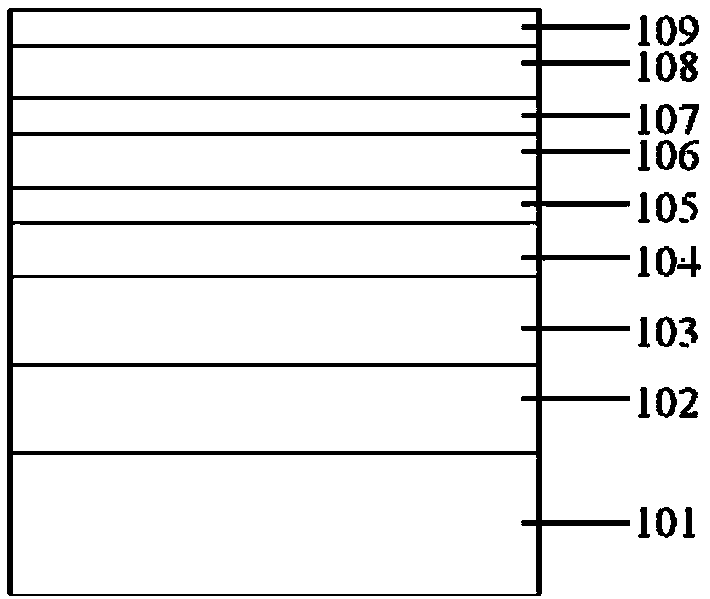
[0132] Embodiment 1 The manufacturing process of a GaN-based blue laser or superluminescent light-emitting diode in this embodiment includes:

[0133] S1: Using metal organic chemical vapor deposition (MOCVD) equipment to grow nitride semiconductor laser or superluminescent light emitting diode structure on GaN substrate, which includes: n-GaN contact layer with a thickness of about 500nm; 100 pairs of n-Al 0.16 GaN / GaN superlattice structure, in which each layer is about 2.5nm thick as n-type optical confinement layer; n-In with a thickness of about 100nm 0.03 Ga 0.97 N waveguide layer; 3 pairs of In 0.16 Ga 0.84 N / GaN multiple quantum wells, where each layer of In 0.16 Ga 0.84 The N quantum well is about 2.5nm thick, and each GaN barrier is about 15nm thick; the unintentionally doped In with a thickness of about 80nm 0.03 Ga 0.97 N waveguide layer; p-Al with a thickness of about 20nm 0.2 Ga 0.8 N electron blocking layer; 150 pairs of p-Al 0.16 a GaN / GaN superlattice...

Embodiment 2

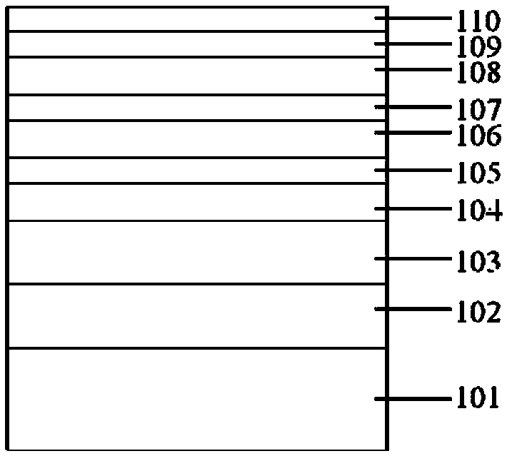
[0144] Embodiment 2 The manufacturing process of a GaN-based near-ultraviolet laser in this embodiment includes:

[0145] S1: Using metal organic chemical vapor deposition (MOCVD) equipment to grow ultraviolet laser structures on Si(111) substrates, including: n-GaN contact layer with a thickness of about 500nm; 120 pairs of n-Al 0.2 GaN / GaN superlattice structure, in which each layer is about 2.5nm thick as an n-type optical confinement layer; n-Al with a thickness of about 80nm 0.02 Ga 0.98 Nn side waveguide layer; 2 pairs of In 0.03 Ga 0.97 N / Al 0.08 Ga 0.92 N multiple quantum wells, where each layer of In 0.03 Ga 0.97 The N quantum well is about 2.5nm thick, each layer of Al 0.08 Ga 0.92 N barrier about 14nm thick; unintentionally doped Al about 60nm thick 0.02 Ga 0.98 Np side waveguide layer; p-Al about 25nm thick 0.25 Ga 0.75 N electron blocking layer; 30 pairs of p-Al 0.16 GaN / GaN superlattice structure, wherein each layer has a thickness of about 2.5nm as ...

Embodiment 3

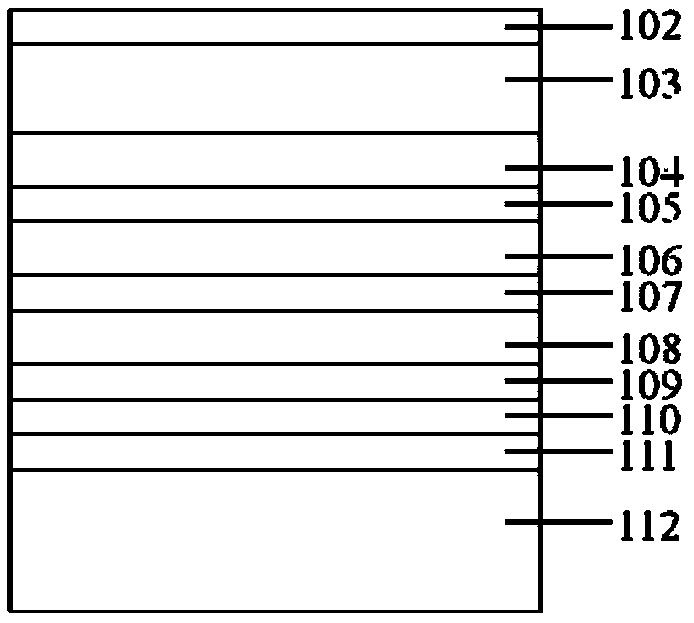
[0158] Embodiment 3 The manufacturing process of an AlGaN-based deep ultraviolet laser in this embodiment includes:

[0159] S1: Using metal organic chemical vapor deposition (MOCVD) equipment to grow deep ultraviolet laser structures on sapphire substrates, including: n-Al with a thickness of about 1000nm 0.45 Ga 0.5 N contact layer; 100 pairs of n-Al 0.65 Ga 0.35 N / Al 0.45 Ga 0.55 N superlattice structure, in which each layer is about 2.3nm thick as an n-type optical confinement layer; n-Al with a thickness of about 75nm 0.45 Ga 0.55 Nn side waveguide layer; 3 pairs of Al 0.35 Ga 0.65 N / Al 0.45Ga 0.55 N multiple quantum wells, where each layer of Al 0.35 Ga 0.65 The N quantum well is about 3nm thick, and each layer of Al 0.45 Ga 0.55 N barrier about 10nm thick; unintentionally doped Al about 60nm thick 0.45 Ga 0.55 Np side waveguide layer; p-Al about 20nm thick 0.65 Ga 0.35 N electron blocking layer; p-Al about 50nm thick 0.45 Ga 0.55 N-contact layer. ref...


PUM


Abstract

The application discloses a nitride semiconductor light-emitting device and a manufacturing method thereof. The nitride semiconductor light emitting device includes an epitaxial structure, the epitaxial structure has a first surface and a second surface opposite to the first surface, the first surface is and located on the n-type side of the epitaxial structure, the second surface is located on the p-type side of the epitaxial structure, the n-type side of the epitaxial structure is in electrical contact with the n-type electrode, and the p-type side is in contact with the p-type electrode are in electrical contact, and the first surface is formed with a ridge waveguide structure. The nitride semiconductor light-emitting device of the present application, especially the III-V group nitride semiconductor laser or superluminescent light-emitting diode has the advantages of low resistance, low internal loss, small threshold current, small thermal resistance, good stability and reliability, etc., and at the same time Its preparation process is simple and easy to implement.

Description

technical field [0001] This application relates to a semiconductor optoelectronic device and its preparation method, in particular to a nitride semiconductor light-emitting device with a ridge waveguide structure, such as III-V nitride semiconductor lasers, superluminescent light-emitting diodes and its preparation method, belonging to semiconductor field of optoelectronic technology. Background technique [0002] III-V nitride semiconductors are called the third-generation semiconductor materials, which have the advantages of large band gap, good chemical stability, and strong radiation resistance; their band gap covers from deep ultraviolet, the entire visible light, to near infrared It can be used to make semiconductor light-emitting devices, such as light-emitting diodes, lasers and superluminescent light-emitting diodes. Among them, lasers and superluminescent light-emitting diodes based on III-V nitride semiconductors have the advantages of simple fabrication, small s...

Claims


Application Information

Patent Timeline
Patent Type & Authority Patents(China)
IPC IPC(8): H01L33/00H01L33/16H01L33/20H01L33/44H01S5/22H01S5/30
CPCH01L33/0045H01L33/0075H01L33/16H01L33/20H01L33/44H01S5/2201H01S5/3013H01S5/22H01L33/0093H01L33/007H01L33/36H01L33/32H01L2933/0016H01S5/2031H01S5/34333H01S5/2086H01S5/0217H01S5/04253H01S5/0234H01L33/58H01S5/2275
Inventor 孙钱冯美鑫周宇高宏伟杨辉
Owner SUZHOU INST OF NANO TECH & NANO BIONICS CHINESE ACEDEMY OF SCI
Why Eureka
Try Eureka