Semiconductor device and method of manufacturing the same

A manufacturing method and semiconductor technology, applied in the fields of semiconductor/solid-state device manufacturing, semiconductor devices, semiconductor/solid-state device components, etc., can solve problems such as difficulty in realizing the miniaturization of electrode pads

Inactive Publication Date: 2018-08-07
TOYOTA JIDOSHA KK
View PDF4 Cites 0 Cited by
  • Summary
  • Abstract
  • Description
  • Claims
  • Application Information

AI Technical Summary

Problems solved by technology

When aluminum spatter occurs, it is dif

Method used


Image

  • Semiconductor device and method of manufacturing the same
  • Semiconductor device and method of manufacturing the same
  • Semiconductor device and method of manufacturing the same

Examples


Embodiment Construction

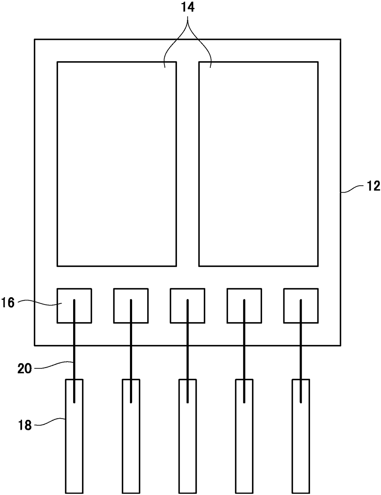
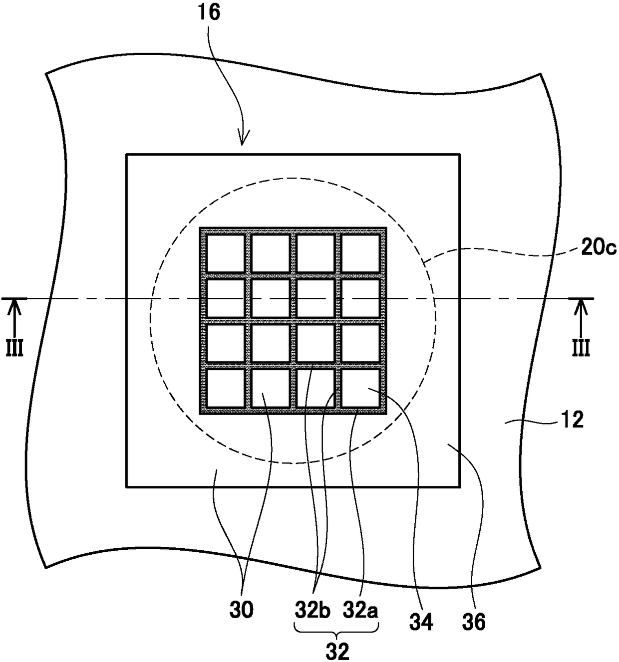
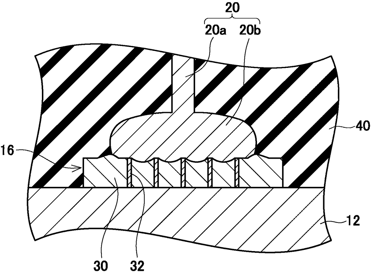
[0023] figure 1 The upper surface of the semiconductor device is shown. The semiconductor device has a semiconductor substrate 12 . The semiconductor substrate 12 is composed of a semiconductor mainly composed of Si (silicon). In addition, the semiconductor substrate 12 may be made of a wide bandgap semiconductor mainly composed of SiC (silicon carbide) or GaN (gallium nitride). Main electrodes 14 and signal electrode pads 16 are provided on the upper surface of the semiconductor substrate 12 . The size of each signal electrode pad 16 is smaller than the size of each main electrode 14 . The main electrode 14 is connected to an unillustrated wiring member by solder. A plurality of pins 18 are arranged on the side of the semiconductor substrate 12 . Each signal electrode pad 16 is connected to a corresponding pin 18 through a lead wire 20 . Furthermore, although not shown, a lower electrode is provided on the lower surface of the semiconductor substrate 12 . The lower ele...


PUM


Abstract

The invention provides a semiconductor device and a method of manufacturing the same. The aluminum splashing is inhibited. The semiconductor device includes an electrode pad provided above a semiconductor substrate; and a wire bonded on the electrode pad and including copper. The electrode pad includes an electrode layer including aluminum and a support layer harder than the wire and the electrodelayer. The wire is in contact with the electrode layer and the support layer. The wire is supported by the support layer, the deformation of the electrode layer is inhibited, and thus the aluminum splashing is inhibited.

Description

technical field [0001] The technology disclosed in this specification relates to a semiconductor device and a manufacturing method thereof. Background technique [0002] Patent Document 1 discloses a technique of bonding copper leads to aluminum electrode pads. Since the lead wire is harder than the electrode pad, the electrode pad is crushed by the lead wire during bonding, and the material constituting the electrode pad is pushed out from the lower portion of the lead wire toward the outer peripheral side. As a result, the electrode pads bulge around the bonding portion. This phenomenon is commonly referred to as aluminum splash. When aluminum spatter occurs, it is difficult to miniaturize the electrode pad. In the technique of Patent Document 1, spattering of aluminum is suppressed by partially providing an interlayer film under the electrode pad. [0003] prior art literature [0004] Patent Document 1: Japanese Patent Laid-Open No. 2012-109419 Contents of the inv...

Claims


Application Information

Patent Timeline
IPC IPC(8): H01L23/488H01L21/60
CPCH01L24/05H01L24/85H01L2224/05624H01L2224/05554H01L2224/02125H01L2224/04042H01L2224/48463H01L2224/45147H01L24/29H01L24/32H01L24/48H01L24/49H01L24/73H01L2224/04026H01L2224/05684H01L2224/05686H01L2224/0603H01L2224/06051H01L2224/06181H01L2224/291H01L2224/32225H01L2224/48453H01L2224/49175H01L2224/73265H01L2924/10253H01L2924/10272H01L2924/1033H01L2224/05552H01L2224/05555H01L2224/05556H01L2224/05578H01L2224/05576H01L24/45H01L2924/35121H01L2224/85205H01L2924/01014H01L2924/014H01L2924/00014H01L2224/05015H01L2224/05076H01L2224/05184H01L2224/05188H01L2924/05442H01L2224/4502H01L2224/05124
Inventor 渡边健雅武直矢儿玉幸雄
Owner TOYOTA JIDOSHA KK
Why Eureka
Try Eureka