Electrostatic discharge device with replaced gate and used for improving maintaining voltage, and manufacturing method thereof

A technology for maintaining voltage and electrostatic discharge. It is applied in the fields of electric solid-state devices, semiconductor/solid-state device manufacturing, and electrical components. It can solve the problems that affect the robustness of the LDMOS structure, uneven fork guide conduction, and the device cannot be turned off. Uneven conduction characteristics, preventing uneven conduction, and easy operation

Active Publication Date: 2018-08-07
HUNAN NORMAL UNIVERSITY
View PDF6 Cites 0 Cited by
  • Summary
  • Abstract
  • Description
  • Claims
  • Application Information

AI Technical Summary

Problems solved by technology

However, because of the Kirk effect of the LDMOS structure, its maintenance voltage will be low, and there is a serious problem of uneven conduction of the fingers, that is, only some fingers are turned on to discharge the electrostatic current, and the rest of the fingers are not in working state, which seriously affects The overall ESD robustness of the LDMOS structure, and it is prone to latch-up problems, so that the device cannot be turned off until it burns

Method used


Image

  • Electrostatic discharge device with replaced gate and used for improving maintaining voltage, and manufacturing method thereof
  • Electrostatic discharge device with replaced gate and used for improving maintaining voltage, and manufacturing method thereof
  • Electrostatic discharge device with replaced gate and used for improving maintaining voltage, and manufacturing method thereof

Examples


Embodiment Construction

[0033] The present invention will be further described below in conjunction with the accompanying drawings and embodiments.

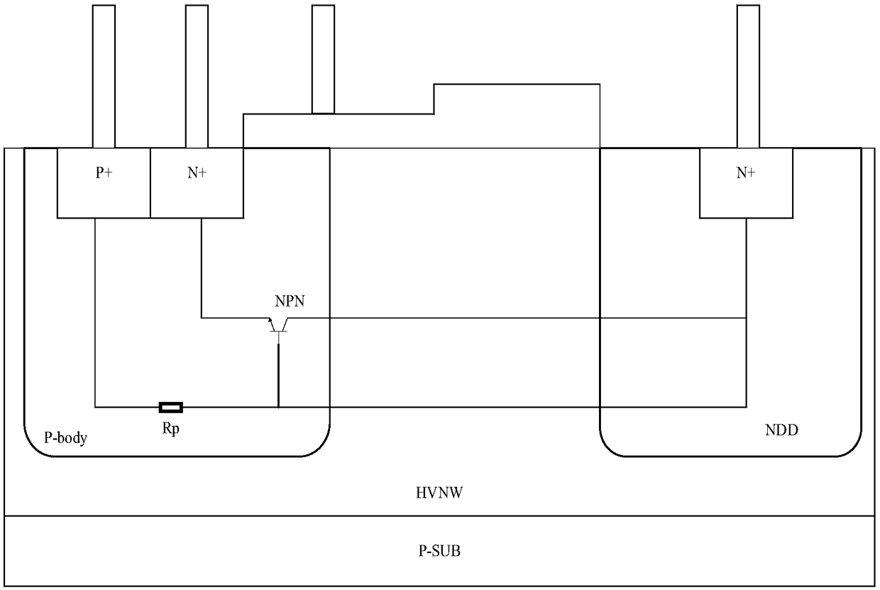
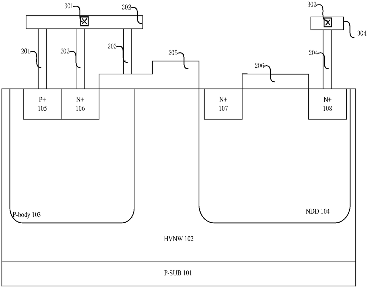
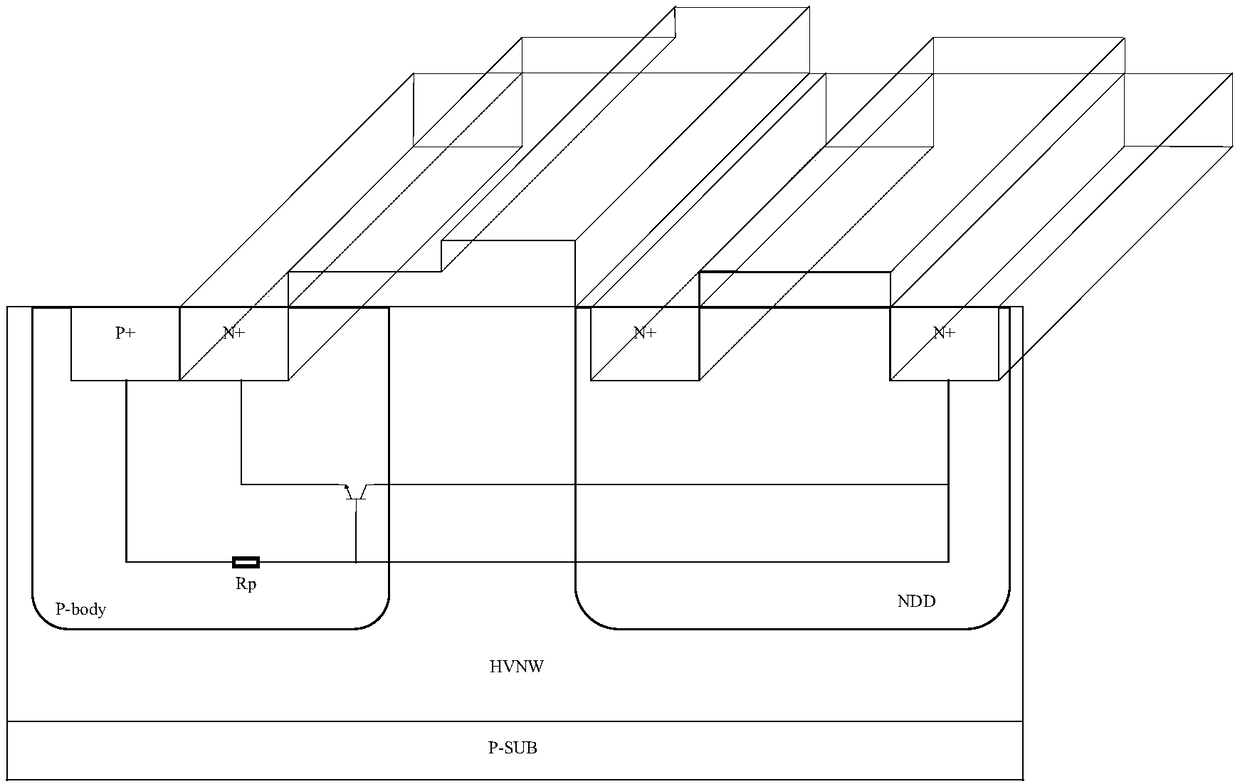
[0034] Such as figure 2 , image 3 , Figure 5 As shown, an electrostatic discharge device with a dummy gate with increased sustain voltage includes a substrate P-SUB101, a HVNW region 102, a P-body region 103, an NDD region 104, a first P+ injection region 105, and a first N+ injection region 106 , the second N+ implantation region 107, the third N+ implantation region 108, the first polysilicon gate 205, the second polysilicon dummy gate 206, the substrate P-SUB 101 is provided with the HVNW region 102, the HVNW region 102 A P-body region 103 and an NDD region 104 are provided in sequence from left to right in the P-body region 103, and a first P+ implantation region 105 and a first N+ implantation region 106 are arranged in sequence in the P-body region 103 from left to right. A polysilicon gate 205 spans between the HVNW region 102 and the P-body ...


PUM


Abstract

The invention discloses an electrostatic discharge device with a replaced gate and used for improving a maintaining voltage; the electrostatic discharge device comprises a substrate having a HVNW zone; a P-body zone and a NDD zone are arranged in order from left to right in the HVNW zone; a first P+ injection zone and a first N+ injection zone are arranged from left to right in order in the P-bodyzone; a first polysilicon gate across between the HVNW zone and the P-body zone; a second N+ injection zone, a second polysilicon replaced gate, and a third N+ injection zone are arranged in order from left to right in the NDD zone; the second polysilicon replaced gate form a polysilicon replaced gate structure so as to improve the device maintaining voltage. The polysilicon replaced gate structure is employed so as to enable the LDMOS device electrostatic discharge to be far away from the surface of a channel zone; most electrostatic current can be discharged from the inner side of the device, so the device can bear ESD pulse stress with enough high intensity, thus preventing the device surface to have thermal breakdown phenomenon.

Description

technical field [0001] The invention relates to the field of integrated circuits, in particular to an electrostatic discharge device with a dummy gate for increasing sustain voltage and a manufacturing method thereof. Background technique [0002] In the past few decades, electronic technology has developed rapidly and orderly. Electronic products have spread in all aspects of people's daily life. The application of integrated circuits has become more and more extensive. Circuit development still follows the direction guided by Moore's Law, with larger devices, higher integration, smaller sizes, and so on. [0003] Electrostatic discharge (ESD) is an important cause of circuit failure in integrated circuits. With the development of semiconductor technology, the importance of ESD protection has become increasingly prominent. According to the statistics of relevant data, in the field of microelectronics, because of ESD phenomenon About 58% of integrated circuits fail, which f...

Claims


Application Information

Patent Timeline
Patent Type & Authority Applications(China)
IPC IPC(8): H01L27/02H01L21/8249
CPCH01L21/8249H01L27/0255H01L27/0288
Inventor 金湘亮汪洋
Owner HUNAN NORMAL UNIVERSITY
Why Eureka
Try Eureka