A kind of superstructure LED chip and preparation method thereof
A technology of LED chips and superstructures, applied in the direction of semiconductor devices, electrical components, circuits, etc., can solve the problems of short service life of vertical LED chips, poor contact between electrodes and substrates, and the bonding surface is not flat enough to improve the effective bonding. performance, shorten the production cycle, and protect from damage
- Summary
- Abstract
- Description
- Claims
- Application Information
AI Technical Summary
Problems solved by technology
Method used
Image
Examples
Embodiment 31
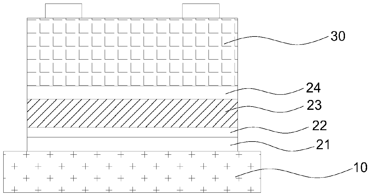
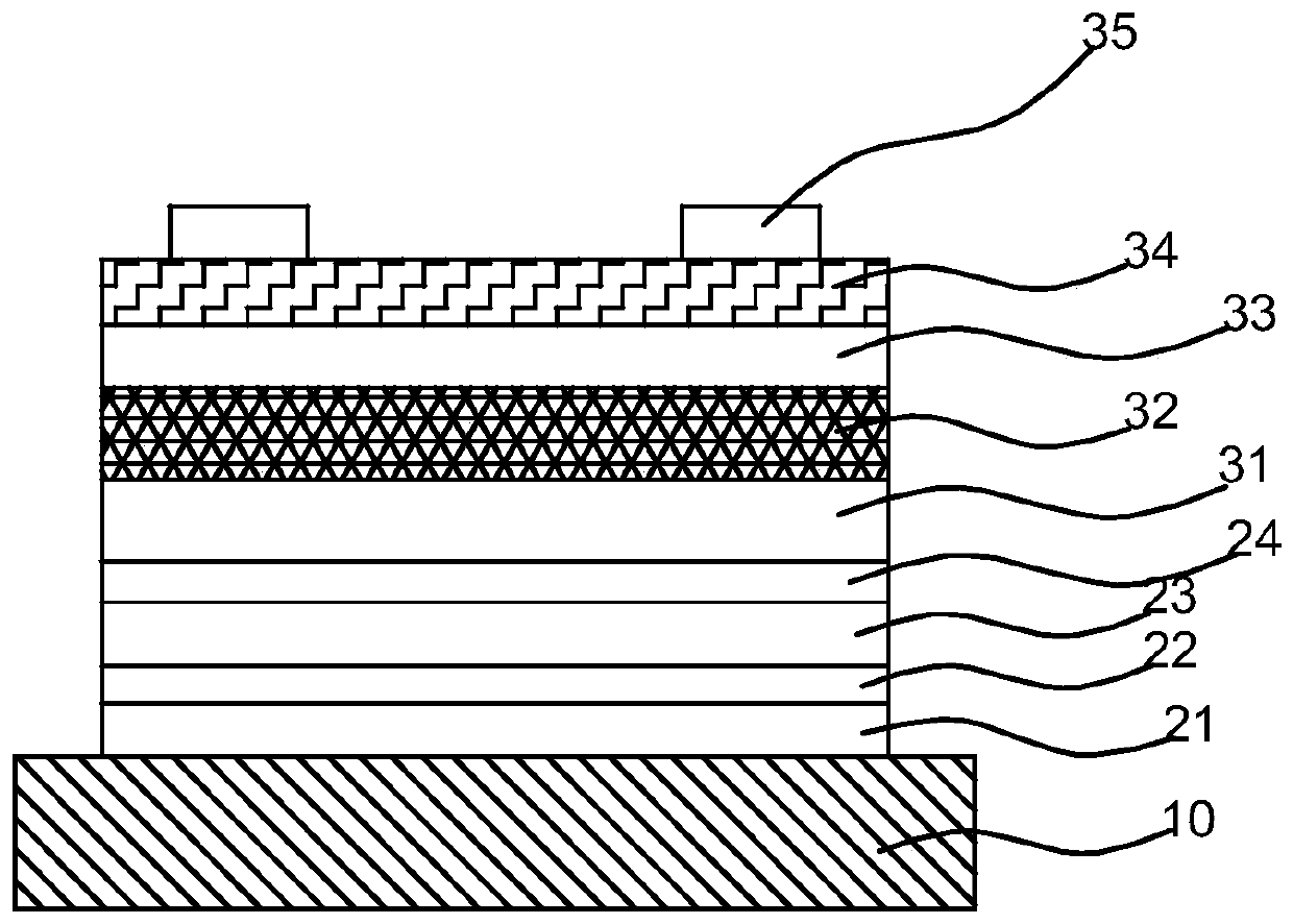
[0051] Step 1: sequentially grow a 300nm-thick AlN buffer layer, a 700nm-thick non-doped GaN layer, a 2000nm-thick n-type GaN layer, a 120nm-thick multi-quantum well light-emitting layer and 200nm thick p-type GaN layer.
[0052] Step 2: On the p-type GaN layer, a 100nm thick Ni / Ag / Ni / Ag reflective layer and a 20nm thick Ti protection layer are sequentially deposited using electron beam evaporation equipment.
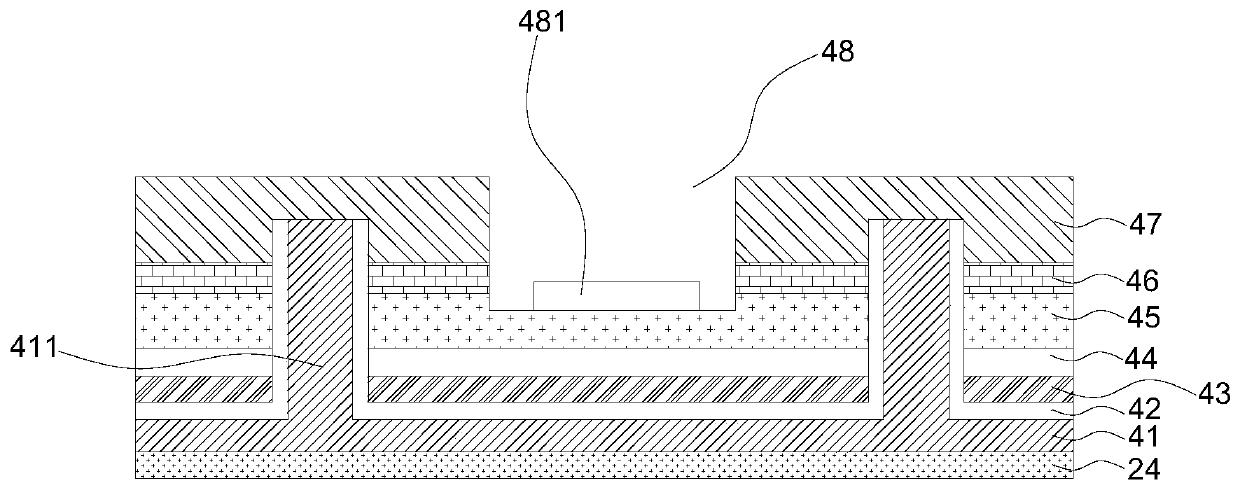
[0053] Step 3: Use ICP etching technology to form a via structure on the Ti protective layer that runs through the Ti protective layer, reflective layer, p-type GaN layer, multi-quantum well light-emitting layer and part of the n-type GaN layer. The bottom of the via structure is located at within the n-type GaN layer.
[0054] Step 4: Deposit SiO with a thickness of 10 μm on the Ti protective layer and in the via structure by PECVD 2 Insulation.
[0055] Step 5: Removal of SiO at the bottom of the via structure using selective acid etching 2 The insulating layer, t...
Embodiment 32
[0065]Step 1: Grow a 1200nm-thick non-doped GaN layer, a 2500nm-thick n-type GaN layer, a 150nm-thick multi-quantum well light-emitting layer and a 200nm-thick p-type GaN layer on the surface of the sapphire substrate sequentially by metal-organic compound vapor deposition technology .
[0066] Step 2: A 400nm thick Ni / Ag / Ni / Ag reflective layer and a 100nm thick Ti protective layer are sequentially deposited on the p-type GaN layer using thermal evaporation equipment.
[0067] Step 3: Use ICP etching technology to form a via structure on the Ti protective layer that runs through the Ti protective layer, reflective layer, p-type GaN layer, multi-quantum well light-emitting layer and part of the n-type GaN layer. The bottom of the via structure is located at within the n-type GaN layer.
[0068] Step 4: Deposit SiN with a thickness of 10 μm on the Ti protective layer and in the via structure by PECVD 1.8 Insulation.
[0069] Step 5: Removal of SiN at the bottom of the via str...
PUM
 Abstract
Description
Claims
Application Information


