Integrated device for amplitude modulation, phase modulation and radio frequency offset

An integrated device and phase modulator technology, applied in the field of circuit integration, can solve the problems of unfavorable cost of various discrete devices, unfavorable improvement of component quality, miniaturization and multi-function disadvantage, etc., to facilitate mass production and promotion, and to facilitate Assembly application, stable and reliable performance

Active Publication Date: 2018-08-14
厚元技术(香港)有限公司
View PDF5 Cites 1 Cited by
  • Summary
  • Abstract
  • Description
  • Claims
  • Application Information

AI Technical Summary

Problems solved by technology

[0004] 1. Debugging is required during assembly, which is not conducive to large-scale production and the intervention of human factors introduces uncertain factors, which is not conducive to improving the quality of the entire component;
[0005] 2. A variety of discrete devices are not conducive to further miniaturization and multi-function of the system;
[0006] 3. A variety of discrete devices are not conducive to further cost reduction

Method used


Image

  • Integrated device for amplitude modulation, phase modulation and radio frequency offset
  • Integrated device for amplitude modulation, phase modulation and radio frequency offset
  • Integrated device for amplitude modulation, phase modulation and radio frequency offset

Examples


specific Embodiment

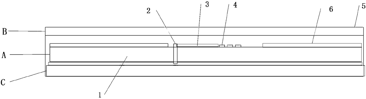
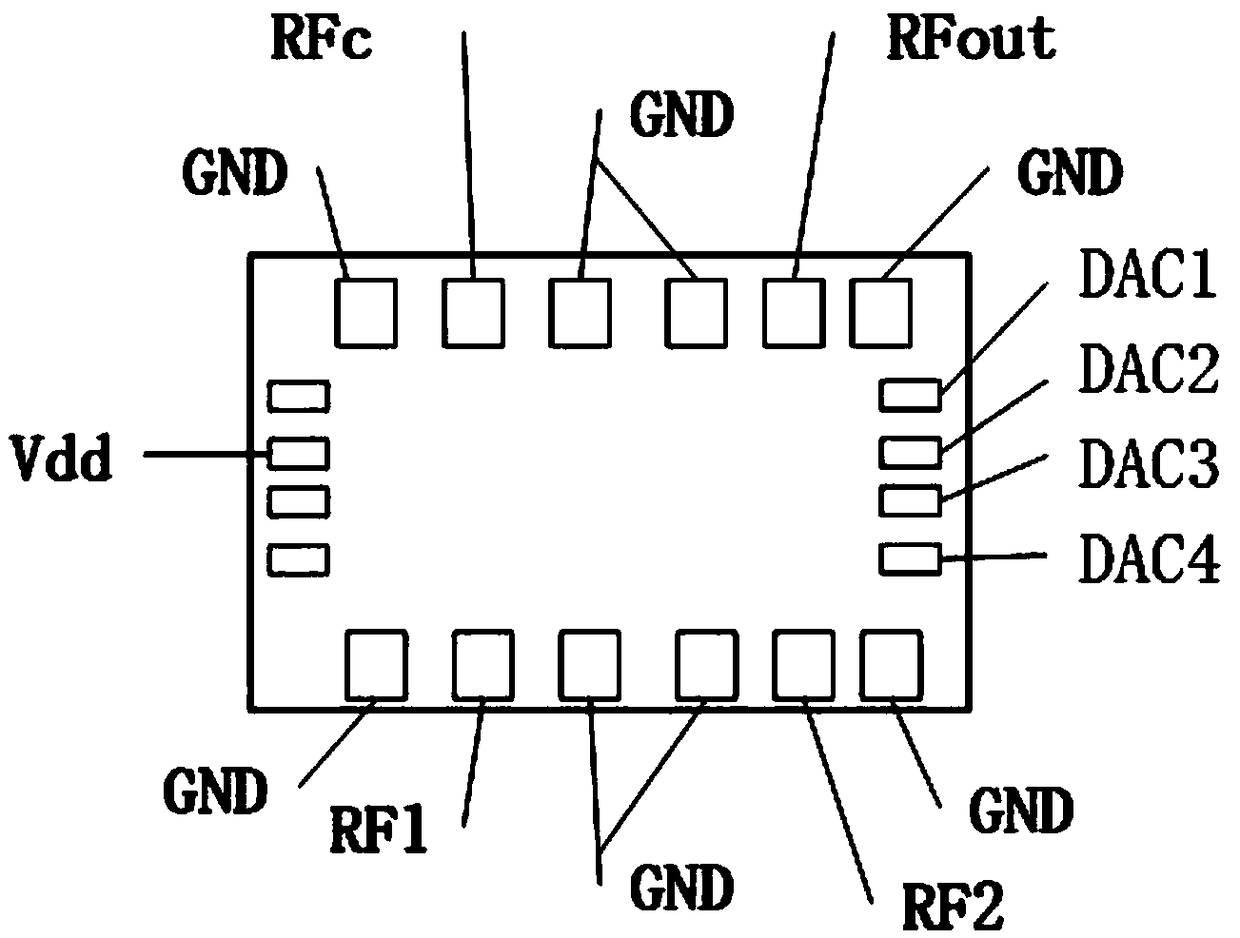
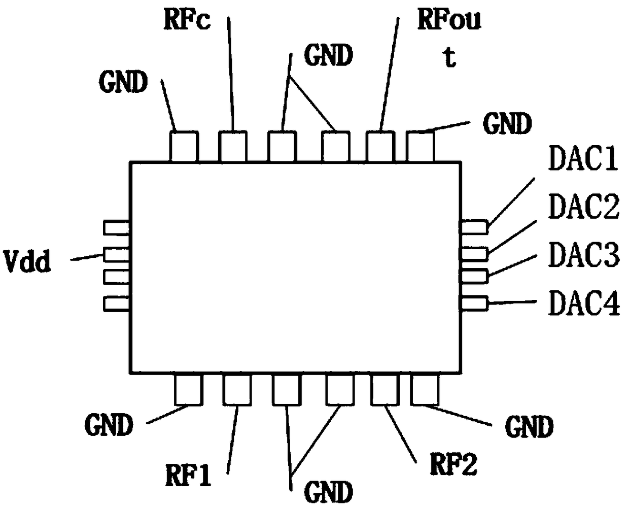
[0055] As an optimization scheme of the embodiment of the present invention, please refer to Figure 2-Figure 5 , The integrated chip includes an external interface; the external interface includes two radio frequency input circuits and two radio frequency output circuits; for ease of description, the two radio frequency input circuits are respectively a first radio frequency input circuit and a second radio frequency input circuit, The two radio frequency output circuits are respectively a first radio frequency output circuit and a second radio frequency output circuit. Wherein, the first radio frequency input circuit is an amplitude and phase modulation circuit, the second radio frequency input circuit is a delayer A1 circuit, and the first radio frequency input circuit and the second radio frequency input circuit are respectively connected to the combiner A4 In addition, the first RF output circuit is a combined coupling circuit, the second RF output circuit is a combined am...


PUM


Abstract

The invention relates to the technical field of circuit integration and provides an integrated device for amplitude modulation, phase modulation and radio frequency offset; the integrated device comprises a middle layer, a substrate located on the lower surface of the middle layer, and a top layer covering the upper surface of the middle layer; the middle layer is integrated into a plurality of functional circuits having amplitude modulation, phase modulation and offset through a medium, a micro-strip and a discrete component; the functional circuit comprises a combiner, a controller, a delayer, a coupler, two or more amplitude modulation devices and two or more phase adjusters, which are in circuit design connection with each other; the top layer is used for packaging the middle layer andshielding electromagnetic interference generated by the middle layer; and the substrate is used for supporting the middle layer and the top layer, dissipating heat of the middle layer, encapsulatingthe middle layer and shielding electromagnetic interference generated by the middle layer. According to the integrated device in the invention, the functional circuit with the amplitude modulation function, the phase modulation function and the radio frequency offset function is integrated in the integrated chip; the integrated device has the advantages of being small in size and high in integration level; meanwhile, an integrated packaging technology is adopted, so that batch production and popularization are facilitated.

Description

Technical field [0001] The invention relates to the technical field of circuit integration, in particular to an integrated device used for amplitude modulation, phase modulation and radio frequency cancellation. Background technique [0002] So far, with the rapid development of communication technology, the fifth-generation communication technology is continuously advancing, and the transmission system is developing at a high speed in the direction of low cost, low power consumption, miniaturization, multi-function, high performance, and multiple modes. [0003] At present, radio frequency transmission systems with cancellation functions are still widely used in communication systems due to their relatively mature technology and better performance indicators. Among them, radio frequency integrated devices are the core units of the cancellation circuit, and the circuit architecture includes amplitude modulators and phase modulators. , Combiners, delayers, couplers and other functio...

Claims


Application Information

Patent Timeline
Patent Type & Authority Applications(China)
IPC IPC(8): H01L27/24
CPCH10B63/00
Inventor 孟庆南
Owner 厚元技术(香港)有限公司
Why Eureka
Try Eureka