Efficient silicon wafer slicing device

A slicing device and silicon wafer technology, which is applied to fine working devices, stone processing equipment, manufacturing tools, etc., can solve the problems of inconvenient disassembly, installation and inspection, negative impact on product yield, low cutting efficiency, etc., to improve cutting efficiency. And the effect of cutting accuracy, easy disassembly, installation and inspection, and improved service life

Pending Publication Date: 2018-08-21
浙江海顺新能源有限公司
View PDF0 Cites 2 Cited by
  • Summary
  • Abstract
  • Description
  • Claims
  • Application Information

AI Technical Summary

Problems solved by technology

[0002] Wafer thickness is a factor that affects productivity. It is related to the number of wafers produced per silicon block. Ultra-thin silicon wafers present additional challenges for wire saw technology, because their production is much more difficult. Except In addition to the mechanical brittleness of silicon wafers, if the wire saw process is not precisely controlled, tiny cracks and bends will have a negative impact on product yield. The ultra-thin silicon wafer wire saw system must be able to control process linearity, cutting line speed and pressure, and cutting cooling. Liquid for precise control
[0003] Regardless of the thickness of the silicon wafer, manufacturers of crystalline silicon photovoltaic cells have put forward extremely high requirements for the quality of the silicon wafer. Both) should be minimized, and the requirements for additional back-end processing such as polishing should also be minimized. The use of slicers is inseparable from the processing of silicon wafers, but the cutting efficiency of existing slicers is low and the cutting accuracy is low. can not be guaranteed, and its complex structure brings inconvenience to people's disassembly, installation and inspection. Therefore, we propose a high-efficiency silicon wafer slicing device

Method used


Image

  • Efficient silicon wafer slicing device
  • Efficient silicon wafer slicing device

Examples


Embodiment Construction

[0027] The following will clearly and completely describe the technical solutions in the embodiments of the present invention with reference to the accompanying drawings in the embodiments of the present invention. Obviously, the described embodiments are only some of the embodiments of the present invention, not all of them. Based on the embodiments of the present invention, all other embodiments obtained by persons of ordinary skill in the art without making creative efforts belong to the protection scope of the present invention.

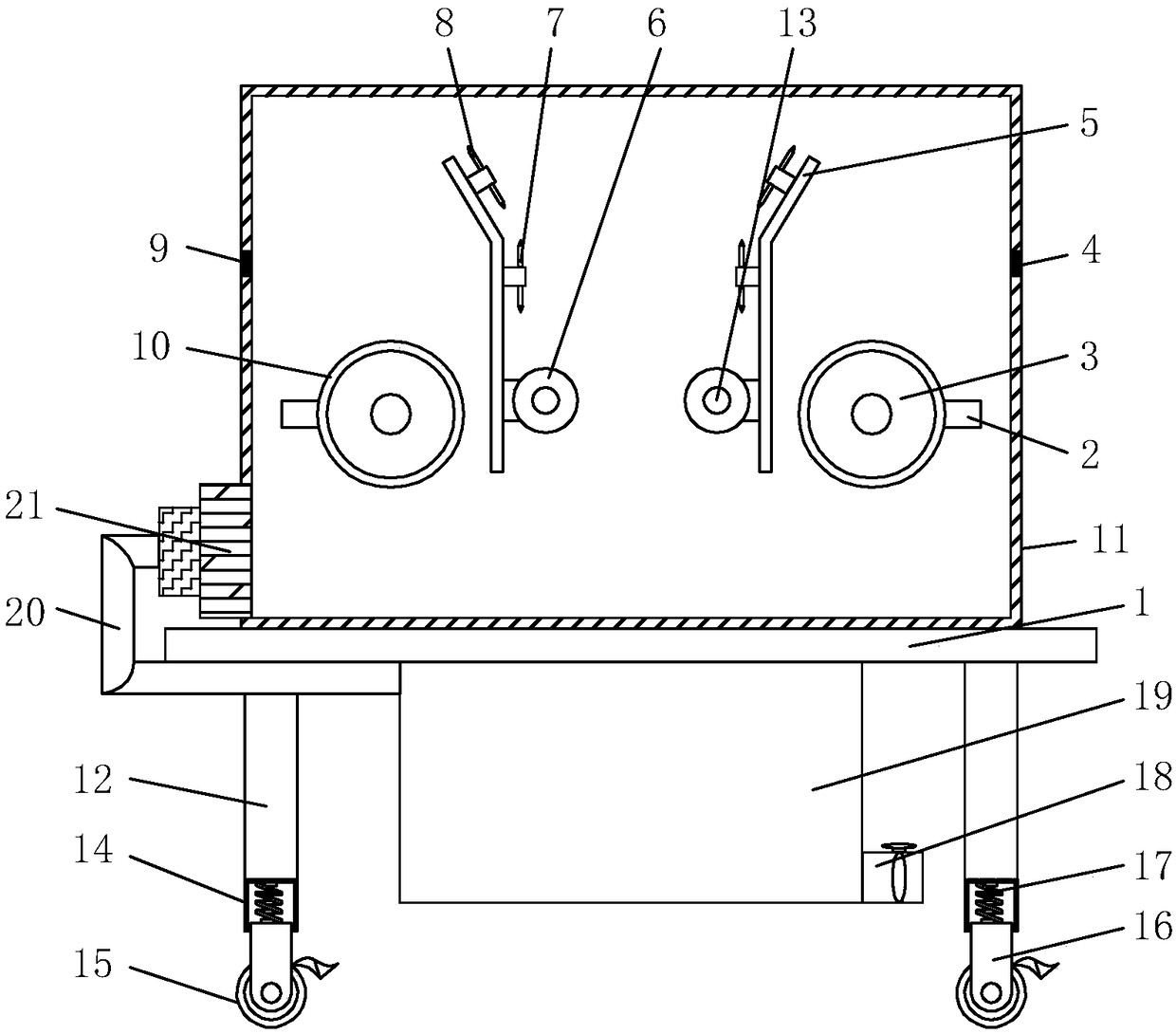
[0028] see Figure 1-2 , a high-efficiency silicon wafer slicing device, comprising a machine tool 1, the middle end of the bottom of the machine tool 1 is fixedly connected with a dust collection box 19, and the bottom of the right side of the dust collection box 19 is provided with a discharge port 18, and the four sides of the bottom of the machine tool 1 are fixed Connected with support leg 12, and the bottom of support leg 12 is fixedly conn...


PUM


Abstract

The invention discloses an efficient silicon wafer slicing device. The device comprises a machine tool, wherein a middle end at the bottom of the machine tool is fixedly connected with a dust collecting box, the bottom of the right side of the dust collecting box is provided with a discharge hole, the periphery of the bottom of the machine tool are all fixedly connected with supporting legs, the bottoms of the supporting legs are fixedly connected with a sleeve, the top of the inner cavity of the sleeve is movably connected with a motion bar through a spring, the bottom of the motion bar is movably provided with an idler wheel, a middle end at the top of the machine tool is fixedly connected with a mounting base, and the lower end of an inner surface of the mounting base is symmetrically provided with retracting rotational shafts. The lower end of the inner surface of the mounting base is symmetrically provided with the retracting rotational shafts, the inner side of a mounting plate is successively and movably provided with a first diamond line slice, a second diamond line slice and a third diamond line slice from bottom to top, the cutting efficiency and cutting accuracy of silicon wafers can be effectively improved, and meanwhile, the slicing device has a simple structure, is convenient to disassemble, assemble and inspect, and conforms to the self-interest of enterprises.

Description

technical field [0001] The invention relates to the technical field of silicon wafer processing equipment, in particular to a high-efficiency silicon wafer slicing device. Background technique [0002] Wafer thickness is a factor that affects productivity. It is related to the number of wafers produced per silicon block. Ultra-thin silicon wafers present additional challenges for wire saw technology, because their production is much more difficult. Except In addition to the mechanical brittleness of silicon wafers, if the wire saw process is not precisely controlled, tiny cracks and bends will have a negative impact on product yield. The ultra-thin silicon wafer wire saw system must be able to control process linearity, cutting line speed and pressure, and cutting cooling. Liquid is precisely controlled. [0003] Regardless of the thickness of the silicon wafer, manufacturers of crystalline silicon photovoltaic cells have put forward extremely high requirements for the qual...

Claims


Application Information

Patent Timeline
Patent Type & Authority Applications(China)
IPC IPC(8): B28D5/04B28D5/00
CPCB28D5/045B28D5/0058
Inventor 季丽王松华聂海洲余志兵
Owner 浙江海顺新能源有限公司
Why Eureka
Try Eureka